Outline#
The goals of this weeks lab are to:
- Understand the basic building blocks of sequential circuits
- Understand the clock input
- Understand the difference between level triggered and edge triggered circuits
- Design a register file which can be used to store/retrieve binary values
Preparation#
Before you attend this week’s lab, make sure:
- You have Digital installed on your computer (if doing the lab remotely)
- You can use Git to commit and push your designs to GitLab
- You are able to design and implement simple combinational logic circuits from a specification
Do an upstream pull to get the latest changes to the lab repository. If you completed exercise 1 of lab 2 the following commands will get the latest changes.
git fetch upstream
git pull --no-ff --no-edit upstream master
You should have the template files for lab 3 with inputs and outputs already defined and tests provided.
Introduction#
So far, all circuits you built were combinational. The output is determined only by the current values of the inputs. However, real-world digital circuits remember and save the state of a system. Such circuits have memory and are called sequential circuits. Sequential circuits may explicitly remember certain previous inputs, or they may summarize the prior inputs in a compressed form called the system’s state. For example, a four-bit binary pattern can store one of the sixteen states for a system. In sequential logic, the output depends on the system’s state in addition to the current inputs.
Consider the two following circuits:
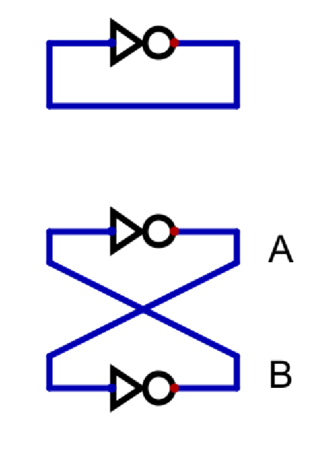
The first circuit is a NOT gate where the gate’s output is fed back into its input. This creates an unstable circuit. Can you analyze why? To analyze the circuit, assume the output of the inverter is HIGH at some point in time. This implies the input to the inverter is HIGH. Therefore, the output is contrary to our assumption (LOW). Indeed, the circuit is unstable and oscillates between two states. A ring oscillator contains an odd number of inverters connected in a chain. The output of a ring oscillator oscillates between HIGH and LOW, and the frequency of oscillation is dictated by the propagation delays of the NOT gates. What happens if we connect an even number of NOT gates in a chain?
The second circuit is similar to the first one but contains two NOT gates connected in a chain. To analyze this circuit, use a process similar to the one we used above. Assume the output on the wire (A) is HIGH. The input to the second NOT gate is, therefore, HIGH. The output of the second NOT gate (B) is LOW. If we follow through with the circuit, we get the same output for A (HIGH) that we assumed. Repeat the thought experiment, but this time consider the output (A) is LOW. And then follow through the circuit. You will find that the output you start with is the same as you finally get. The circuit has memory! It retains the state it is in at any point. This circuit has two stable states: (1) A is HIGH, B is LOW, (2) A is LOW, B is HIGH.
These are two examples of sequential circuits with feedback loops. Although the circuit with two inverters connected in a feedback loop can store one bit of state, unfortunately, we cannot control what the specific state (HIGH or LOW) is via an explicit input terminal. We also cannot control when the state changes. The following circuits will fix these shortcomings.
Exercise 1: SR Latch#
We want a circuit that can store a single bit of information. The second
circuit above has two stable states (HIGH or LOW) and thus stores a single bit.
We can either read A or B (they are complements of each other). The feature we
are looking for is the capability to switch between states. The SR latch offers
this feature because it has two inputs: one which sets (S) the state of
the circuit to output a HIGH value and one which resets (R) the state to
output a LOW value. A possible implementation for the SR latch has been
provided in sr_latch.dig.
You need to recall the truth table for the NOR gate to demystify the behaviour of the SR latch.
Open the design in Digital and experiment with it. Can you analyze the circuit? Note that when the two inputs are LOW the circuit behaves just like the two connected NOT gates above. If you set S or R to HIGH, what is the new state of the SR latch? Analyse the circuit and convince yourself that this works. This is a good place to check in with your tutor if you are unsure or want to make sure that you understand everything.
The truth table for the SR latch is as follows
When
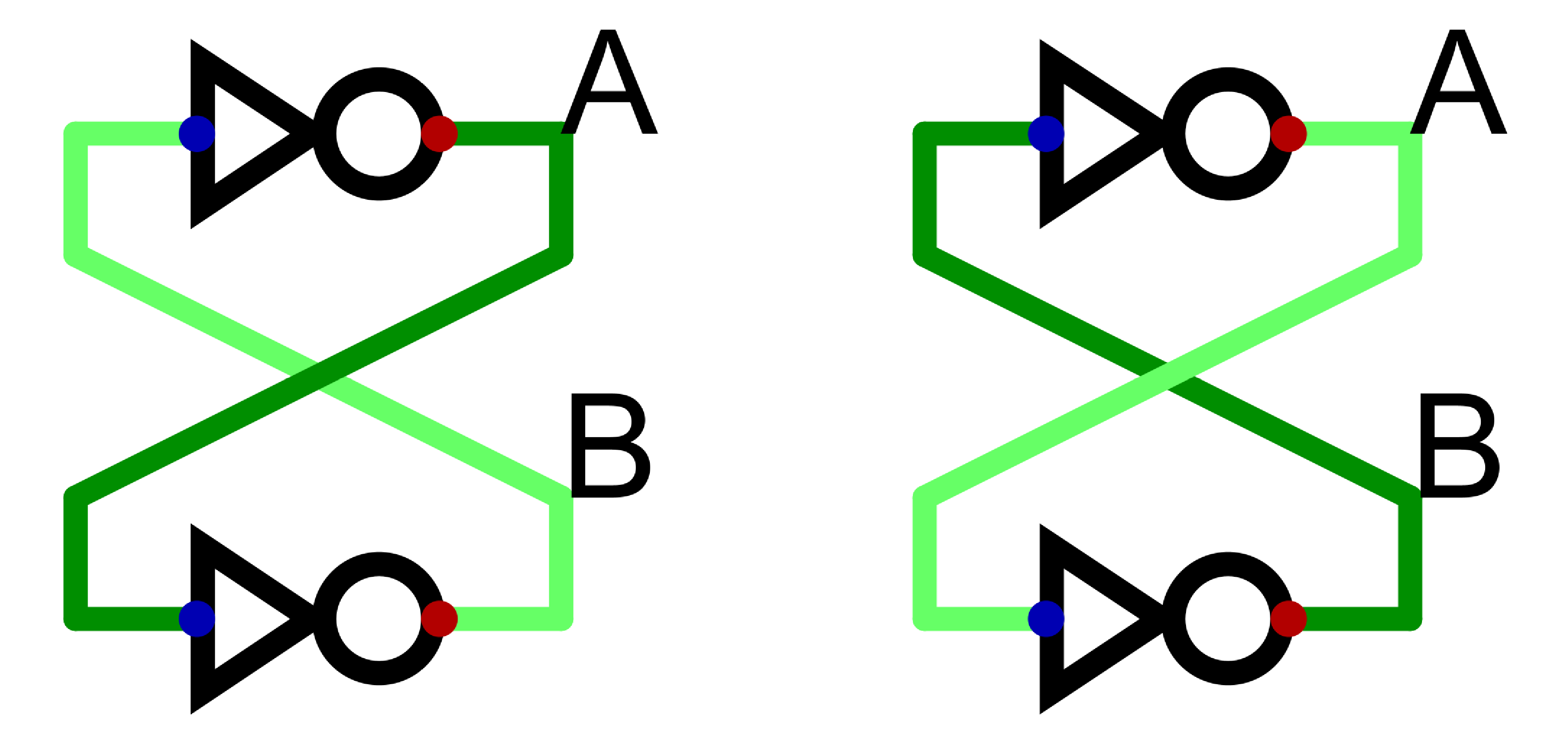
You can switch to drawing diagonal lines by pressing d. Drawing diagonal lines is often considered poor design practice and should be used sparingly. One of the few times it is used is to show the symmetric feedback in this sequential circuit.
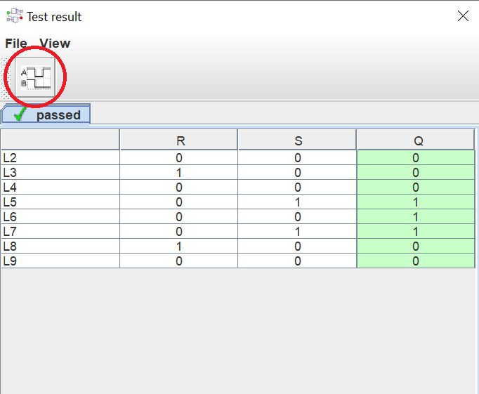
For sequential circuits, the output depends on the previous state. For instance, we can set (or reset) the SR latch and then make the S and R inputs LOW. The output of the latch depends on whether S or R was HIGH previously. In such cases, simply testing the truth table for functional correctness is insufficient. We need the ability to track the circuit’s behaviour over time. To see a timing diagram in Digital, click on the button in the top left of the testing window (see the picture below). This diagram shows how the values of the various inputs and outputs of the circuit change over time. This can better represent the fact that the output depends on the history of the system.
There are many different designs for the SR latch. Can you come up with a different one with similar behaviour?
Exercise 2: D Latch#
The SR latch behaves strangely when both S and R are HIGH. Furthermore, the S and R inputs decide the (future) state of the SR latch and when that state changes (i.e., instantly). Designing sequential circuits becomes more manageable when we separate the concerns of what and when.
The D latch has the following inputs:
We say the latch is ‘transparent’ when
Design a circuit that meets the above specifications. Designing sequential
circuits from scratch can be difficult. Can you create a combinational circuit
in front of the SR latch that transforms
Complete and test d_latch.dig
Exercise 3: Clocks#
Now that we have seen circuits that can store the state of a system, we want
the ability to periodically update the state. So far, we have used an Input
component connected to the enable wire of our D latch and toggled it manually.
Digital has a second type of input called a Clock Input. This component
acts as any other standard input. You can manually click it to toggle its state
and create an input when using your circuit in a larger design. However, the
difference is that it produces a periodic signal that regularly switches
between HIGH and LOW. In real-time, the clock component produces a periodic
square wave. Typically, there is only ever one of these components in a
circuit.
Typically, a clock in digital electronics does not refer to something that provides an absolute value of time. Instead, it is a circuit component that produces a stable (and regular) periodic signal over time. It is used to synchronize sequential elements in digital circuits. Designing circuits with combinational and sequential elements is much easier if we can synchronize all the elements to a single clock input.
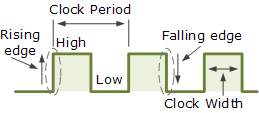
The clock period (or cycle time) is the time between the rising edges of a clock signal. The reciprocal of cycle time is clock frequency. For now, remember that increasing clock frequency increases the work a digital system can accomplish. Note that we will not go into the low-level details of how the clock signal is produced in this course.
Open incrementer.dig. This circuit uses four D latches you designed in the
previous exercise to store a 4-bit number. The input to the latches is fed by
an adder, and the output of the latches goes back to the input of the adder.
The other adder inputs are selected to just add one to its input
If you expected the circuit to break when we tried to advance the clock, well done! If not, can you see why the circuit breaks when the clock line is HIGH? Hint: think about the behaviour of a D latch when the enable line is HIGH. Clearly, what we have is not quite useful enough. We want a circuit that changes its state only at specific instants in time.
We say that the D latch is level-sensitive or level-triggered because whether
it latches the input or not depends on the level (HIGH or LOW) of the enable
(clk signal transitions
from LOW to HIGH. The flip-flop is sometimes called edge-triggered.
Open d_flipflop.dig. To implement the D flip-flop, we can use a pair of D
latches in series with the output of one connecting to the input of the next.
The important part is how the clk input is fed to the two flip-flops. The
clk input to one of the flip-flops is negated. Thus, only one of the latches
is enabled (transparent) at any time. The first latch in the series acts as
a master and the second one acts as a slave. When the master latch is
transparent (input flows to the output), the slave is locked (blocks the input
from flowing to the output). When the rising edge of clk arrives, the master
is locked, and the slave is transparent. In other words, when the clock
switches from LOW to HIGH, the first latch is locked and outputs whatever its
input was to the second latch, which is now transparent.
Experiment with this design to make sure you understand what’s going on. Do
check in with your tutor and make sure you understand everything. What would
happen if you attached the NOT gate to the clk input of the other latch?
Once you have fully analyzed the D flip-flop design and convinced yourself that
it would work, go back to incrementer.dig and replace all the latches with
flip-flops. Does the circuit now behave as intended?
The inputs should be in the same order, the clk input of the flip-flop
replacing the en input of the latch. If this is not the case you can reorder
the inputs of a circuit. Go to Edit -> Order Inputs and make sure the order
is as follows: clk, D. You can select an input and then use the arrows to
change the ordering.
Add an enable line to your D flip-flop. When the enable line is HIGH, the
flip-flop should behave as an ordinary flip-flop. When the enable line is LOW,
the flip-flop should not update its output at the clock edge. Save your design
in d_flipflop_with_en.dig. You can reuse your basic D flip-flop design and
just add some additional logic. Verify your design with the tests provided.
So far we have been storing 1 bit values. To store more bits we can just add
more D flip-flops and connect the control lines (clk and en) together.
In particular, we want a component that can store a 16-bit value
for future labs. This component is called a register. A register can
store a group of bits and binary numbers and patterns. Designing this component
is tedious as it doesn’t contain any additional logic, just wire splitters to
separate each individual wire from the 16-bit input. We have provided this
design in register.dig. It uses 16 copies of your D flip-flop (with enable line)
that you designed in the previous exercise.
Check that the inputs for the individual D flip-flops are in the correct order.
From top to bottom, they should be clk, D, en. If you used the template
file provided and didn’t add or delete any inputs, you should be fine.
This register component is almost identical with the register component in the Digital component library. The only difference is that the Digital registers are always initialised to zero, whereas your register starts with a random value (it just depends on the initial state of all the SR latches at start-up time).
Counter#
Open the file counter.dig. Design a circuit that increments a register each
clock cycle. If the
Exercise 4: Testing Sequential Circuits#
Since sequential circuits depend on the current input and past inputs, we can’t just enumerate all possible inputs as we did for combinational circuits. Tests for sequential circuits look more like a computer program, where we can specify the inputs, toggle the clock line, and then check if the new outputs match what we expect.
If a c is encountered in a test, all the other values are set as the test
describes, and then the signal associated with c is toggled (switched from
LOW to HIGH, and then back from HIGH to LOW). The test is then checked against
for correctness. This means that we can write a test where we can set some
control signals, toggle the clock line, and then check the expected result.
For example, the provided tests for the previous exercise check that the
counter starts at zero then increases by one each clock cycle.
clk ld D Q

0 0 0 0
c 0 0 0x1
c 0 0 0x2
This test assumes that you have used the built-in register component rather than the one given to you as it tests that the counter starts at zero, not some random value.
Write additional tests in for your circuit in counter.dig to check that the ld input works as intended.
Exercise 5: Register File#
Now we have a register that can store one 16 bit value. We can replicate the register components to store more than one single binary number (value). We also want a way to interact with them as a group. For example, we may want a way to choose which register will output its value to a shared output line or which register will read a shared input and update its value. This group of registers and the circuitry to control them as a group is called a register file.
In digital circuits such as register files, ports communicate values in and out of the circuit. For instance, we need a read port in the register file to read the contents of one of the many register. Specifically, we need an address port to specify the register number we want to read. The contents of the specified register are output on the (read) data port. The context typically clarifies if we are talking about the address or data port or the read port in general.
-
A read port consists of one (address) input to specify which register we want to read from and one (data) output to provide the contents of that register.
-
A write port consists of three inputs; a select input to specify which register we want to write to, a data input to provide the data we want to write and a write enable input to signal whether we write anything at all or leave the contents the same.
Register files can have as many read and write ports as necessary. The register file you will design will have two read ports and one write port.
Open reg_file.dig. The register file you will design will have five 16-bit registers.
You should use the register component built into Digital (Memory -> Register) instead of the register component provided in the previous exercise. It has better integration with the testing features built into Digital and predictably initialises to zero when starting the simulation.
The inputs and outputs of the circuit are explained below.
-
RS1(3-bits): Read Select 1, Chooses which register to send to the first outputOUT1. -
RS2(3-bits): Read Select 2, Chooses which register to send to the second outputOUT2. -
WS(3-bits): Write Select, Chooses which register to write to on the next positive clock edge. -
WE(1-bit): Write Enable, If HIGH, the register specified byWSwill be written to on the next positive clock edge. -
IN(16-bits) the data to be stored. -
CLK(1-bit) clock line. -
OUT1(16-bits) the value of the first register selected. -
OUT2(16-bits) the value of the second register selected.
The select inputs use three bits because that is the minimum number of bits needed to represent five different values (to differentiate between our registers). In fact, with three bits we can have up to eight unique values. We only use the first five in this exercise, the other three we leave undefined at this point (in other words, you can make the circuit do whatever you want when the select lines are outside of the 0-4 range). Next week, we will do something with these extra slots.
Hints:
- Look through the inputs and outputs and work out which are used to implement each port of the register file.
- The logic related to reading from and writing to the registers is unrelated and can be designed separately. If you are struggling start with the logic to read from a register, consider the circuits we have looked at in previous labs, they might be useful.
- Have a look at the Demultiplexer and Decoder components (under Plexers) as these may help. Remember you can right-click a component to bring up the component settings and click help to get an explanation of what a circuit does and what the inputs and outputs are.
Complete and test reg_file.dig.
The register file you have designed has two read ports and one write port, allowing two registers to be read at the same time but only one register to be written to each clock cycle. Add a second write port to allow two separate registers to be written to separately on each clock cycle. This is a tricky extension so if you don’t get it right a way that’s fine, you can come back to it later.
Special Case Registers#
You will use this register file in future labs to design a complete processor.
In preparation for that, add the following feature to your register file: when
reading register 000 the 16-bit constant 0 should always be returned. Any
writes to register 000 should be ignored.
The final register file that you have designed should conform to the following specification. This will be important next week when we start bringing everything together.
| Code | Mnemonic | Meaning | Behaviour |
|---|---|---|---|
| 000 | RZ |
Zero Register | Always read zero, writes have no effect. |
| 001 | R1 |
Register 1 | General purpose register. |
| 010 | R2 |
Register 2 | General purpose register. |
| 011 | R3 |
Register 3 | General purpose register. |
| 100 | R4 |
Register 4 | General purpose register. |
| 101 | - | undefined | Read and write is undefined. |
| 110 | - | undefined | Read and write is undefined. |
| 111 | - | undefined | Read and write is undefined. |
Don’t worry about the mnemonics right now. They are just more human-friendly ways of referring to the registers.
Modify your register file to add this special case zero register in slot 000. Ensure that you have pushed your work when
finished, this circuit is one of the assessable deliverables for this lab.
While it may seem silly to lose the use of one of our registers and just return a constant value this has some implications for the design of the processor. Think about why it may be useful to keep a constant value in a dedicated register. What other dedicated uses could registers have?
Exercise 6: Memory#
The register file you have designed could store a maximum of 8 16-bit numbers
(7 if you have completed Exercise 5). What if you want to
store more than that? We could make the register file bigger by adding more
registers but this is not the approach modern computers take. Instead computers
separate out registers and the memory system. The memory system is many orders
of magnitude larger than the register file. In this course, we will use memory
with 16-bit selection lines giving us
Digital has some components that contain all the logic necessary for a memory system so that you don’t need to design it or worry about these complexities. Have a look at the components under Memory -> RAM to see what is available to you. You will use some of these components next week.
If we have a huge memory that we can treat as a large register file why do we need registers at all?