Introduction#
In this week’s lab you’ll read and write some of the special hardware registers on your microbit to see LED “output” from your program. Seeing stuff happen in the real world is a big part of the fun of microcontrollers, so this is going to be fun.
We will be using the lab-08 folder of the lab repo you forked
and cloned in week 7. If not,
here’s a link.
Task 1: Bit Shifting Practice#
Parts of this exercise have been covered previously, but it’s good to get a refresher before diving into the rest of the lab.
Bit-Shifting & Logic Ops#
You will need to use some logic operations in this lab, in particular, setting
(set 1) and clearing (set 0) bits. This warm up exercise gives you a chance
to practice bit shifting and using logic operations to set and clear bits.
The logic operations you need are the bitwise operations OR, AND and XOR, which are useful for manipulating bit vectors because, due to their bitwise nature, you can target specific bits to modify. Specifically, ORRing any bit with 1 will set it (change it to 1), ANDing any bit with 0 will clear the bit (change it to 0) and XOR any bit with 1 will toggle it (flip its current state).
ARM also provides you the bic bit clear instruction, which ANDs a value with the negation of the second
value, which is easier to use when you’re clearing a subset of the bits in a value (your second value just
needs to have 1s everywhere you want to clear)`.
Edit your main.S file so that it looks like the following. Don’t forget the
required .syntax unified and .global main statements at the top of the
file.
main:
  ldr r0, =0xcafe0000
  ldr r1, =0xffff

  @ your code goes here

@ when it's all done, spin in an infinite loop
loop:
  nop
  b loop
| Decimal | |
| Hex | |
| Binary |
Using only the instructions in the Logic and Shift/Rotate subsections of the cheat sheet (but as many registers as you need) write a program which puts all of the following values into the listed registers. Use the cheat sheet and the converter widget to help you out—draw “bit pattern” pictures on a piece of paper if it helps.
0xcafeffffintor30xcafeintor40xcaff0000intor50xc0fe0000intor6
Copy the code into tasks/task-1.S. Commit and push your changes with the message “completed task 1”.
Task 2: Using Labels#
Labels and Loading Arbitrary Numbers into Registers#
Labels are the symbols in your source code followed by a colon
(:), e.g. main:. You’ve probably already got an intuitive feel for how they
work: you put them in your code wherever you like, and when you want to branch
to that part of the program you put the label in as the “destination” part of
the branch instruction. Here’s an example:
loop:
  nop
  @ do stuff

  b loop @ branch back to the "loop" label
In the week 7 lab you even used conditional branches to only branch under certain conditions (i.e., if certain flags were set).
But what are labels, really? Add this code to your main.S file:
.syntax unified
.global main

.type main, %function
main:
  nop
  ldr r0, =an_array


end_check: @ <-- don't remove this label
  nop
inf_loop:
  nop
  b inf_loop

.data
an_array:
.word 0x59d2d9d8, 0x3e682394, 0x5a832dcb, 0x821c34ae
another_array:
.word 0x00000000, 0x00000001
After you step through this line, what’s in r0? You might be wondering what
the = sign is doing in your program. Remember that
instructions are stored in memory with various encodings (some are 16-bit, some
are 32-bit) and that when you use an immediate value constant (e.g. 42) in
an instruction which supports it then the bit pattern for 42
(which is 0b101010) is stored inside that instruction.
This means that if you need to include a constant which is 32 bits long (e.g.
0xABCD1234) then you can’t fit it in the instruction. You may have run into
this problem already—the error message will be something like
Error: invalid constant (ffffffffabcd1234) after fixup
and what it means is that the constant value you’re using is too big (too many bits) for the instruction you’re trying to fit it inside.
If you’re curious about what constant values you are allowed to use, see the Extension Task at the end of this lab.
Because this is a bit of a pain, the assembler provides a special syntax for
storing larger values in registers. It’s based around the ldr (load register)
instruction, and if you prefix the constant with an = sign then the assembler
will generate the code to load the full value into the register.
So how does this relate to the ldr r0, =an_array instruction above? Well, the
answer is that the labels in your program are just values—they’re the
addresses (in your board’s memory space) of the instruction which occurs after
them in the program. After the linker figures out exactly which address each
label points to, it “replaces” them in the program, so that
ldr r0, =an_array
becomes something like (this is not the address that an_array will actually
have)
ldr r0, =0x80001c8
or whatever address the an_array label ends up pointing to (which may change
every time your program changes).
And since 0x80001c4 (or whatever it is) is just a bit pattern in a register,
you can do the usual arithmetic/logic stuff you can do with any values in
registers:
Write a small program which calculates the size (in memory) of an_array. For
this exercise we will define the size of an_array as the total number of bytes
taken up by all individual elements of the array. The resulting size should be
stored in register r1.
While this is easy enough to work out in your head, you should try and load the address of different labels to determine the total size.
Copy your code into tasks/task-2.S, then commit and push your work to GitLab.
The CI will run a test to check you have completed this tasks successfully.
Task 3: The Load-Twiddle-Store Pattern#
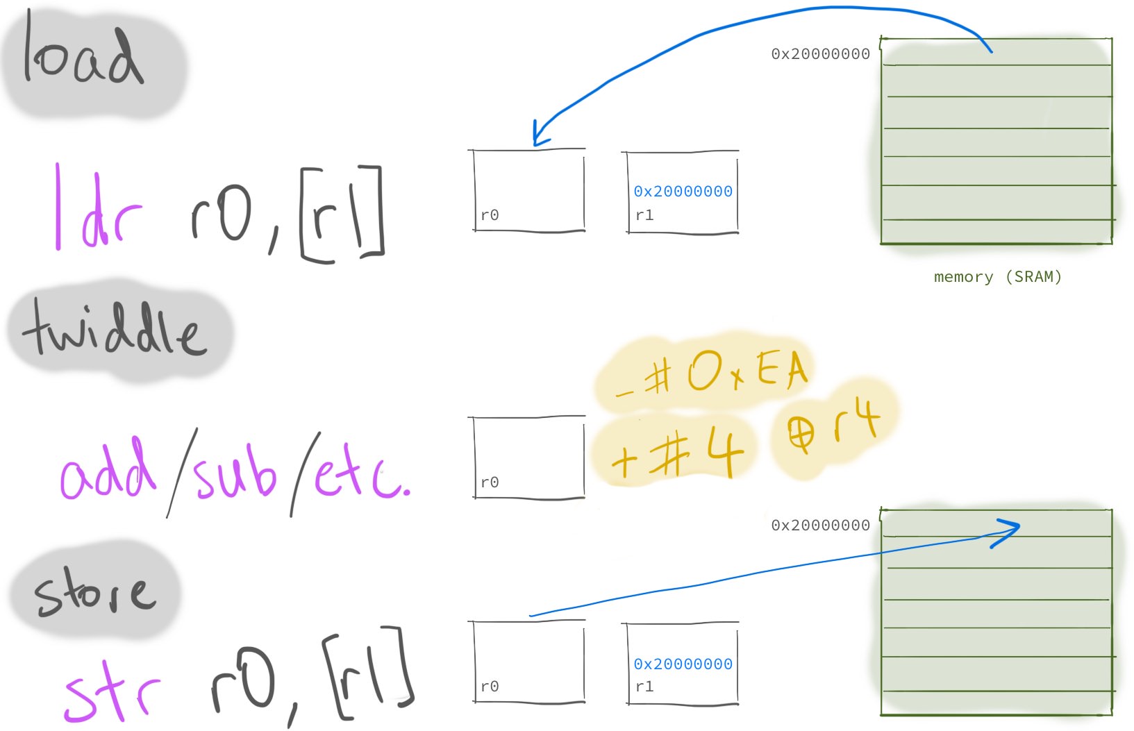
The load-twiddle-store pattern is a fundamental pattern in making your microbit do useful work. The basic idea is this:
- load some data from memory into a register
- operate on (“twiddle”) the value in the register (e.g. with an
addorandinstruction) - store this new value from the register back into memory

Let’s now make use of a data section to store some (spoilers) data, and attempt to load-twiddle-store.
.syntax unified
.global main

.type main, %function
main:
  ldr r1, =storage
  @ your code starts here

end_check: @ <-- don't remove this label
  nop
inf_loop:
  nop
  b inf_loop

.data
storage:
  .word 2, 3, 5, 0 @ don't change this line
Starting with the code above, use the load-twiddle-store pattern to change
the first four data words to 2 1 7 1 instead of 2 3 5 0. Hint:
first load the storage label using the = instruction, then remember that you
can load and store with an offset from this base address
(check the cheat sheet).
You’ll probably also want to use the memory browser view (like you did in week 7) to watch the values
change in memory.
Note that while you can simply store immediate values and skip the “load” part of the “load-twiddle-store” pattern here, you should still do it anyway.
Copy the code from your load-twiddle-store program into tasks/task-3.S.
Commit and push your changes with the message “completed task 3”. The CI will
run a test to verify you have completed this task successfully.
Task 4: Hello, LED!#
You will not be able to complete the following task on the Microbit Emulator. If you have not acquired a physical Microbit yet, now is the time to do so.
So what does all that stuff have to do with blinking the LEDs? Well, the answer
is that there’s a section of the microbit’s address space (0x40000000 to
0x5FFFFFFF) which is mapped to peripherals (as shown in the memory map in last
weeks lab).
To interact with the LEDs, speaker, microphone etc. on the board you need to talk to the hardware by reading and writing to special memory locations in this memory range. To figure out exactly which addresses are mapped to which peripherals, you need to look at the microbit reference manual

One type of peripheral is a General Purpose Input/Output pin. You can see them on your microbit as little gold-coloured contacts at the bottom of the board. Your microbit has lots of them, and you can wire them up to other devices (e.g., sensors, lights or motors) to make more sophisticated systems.
This exercise is pretty long, so here are the steps you’ll go through to turn on an LED:
- figure out which pins are connected to the LED you want to turn on
- set the pins direction to output
- set a bit in the pin’s output data register to turn the LED on
Don’t worry if you don’t understand some of those terms—the rest of this exercise will explain all the details.
Pins and Memory Addresses#
Some of the GPIO connections from microbit’s CPU are already connected to certain bits of hardware on the board. The microbit V2 pinmap explains exactly where each GPIO pin is connected.
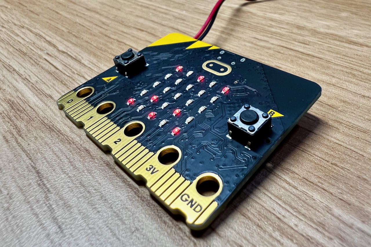
As you can see on your microbit, the LEDs are arranged in a 5x5 array. There’s actually only one pin for each row and and one for each column. The second line of the pin map says that “P1.05” is allocated to COL4. We can read this as “Port 1, pin 5 is allocated to the the 4th column of LEDs.
What GPIO port+pins do you think the top left LED is connected to?
The GPIO pins are grouped into 2 ports (port 0 and 1) and each port has up to 32 pins. It’s worth pointing out that the pin numbering starts at 0, so the first pin in port 0 is P0.0.
| Port | Pins |
|---|---|
| 0 | 0-31 |
| 1 | 0-9 |
Each GPIO port has special configuration registers that allow you to set up and use each pin. GPIO pins support both sending data (setting a voltage to high or low) and receiving data (reading the voltage on the pin as a 0 or 1).
The GPIO registers are not like the CPU registers you’ve been using so far
(e.g. r0 or r5). These registers are mapped to certain parts of the address
space (they’re sometimes called memory-mapped registers). Read/write access to
these registers happens through load/store instructions to a specific memory
address (as with pretty much everything in a load/store architecture).
The memory locations and descriptions of all these registers is in the MCU reference (6.8.2 p 144), there’s a lot of information over those pages, so we’ll copy in some of the information below that is needed for this lab.
The first important piece of information is the base address for each GPIO port’s configuration registers:
| Port | Base Address |
|---|---|
| P0 | 0x50000000 |
| P1 | 0x50000300 |
Now we can find each configuration register at certain offset from these base addresses. Here’s a few that we will use today:
| Register | Offset | Description |
|---|---|---|
| OUT | 0x504 |
Write GPIO port |
| DIR | 0x514 |
Direction of GPIO pins |
So reading these two tables together, if we want to write some data to a pin in
GPIO Port 0, we will need to store a value in the memory address found at
0x50000000 + 0x504 (base + offset).
But how do we write data to a specific pin? Well port 0 can address 32 pins, and the OUT register has 32 bits, so each pin can be changed by setting the value of a specific bit in the OUT register for Port 0 (see the MCU reference, 6.8.2.1 to see how this is described in the manual).
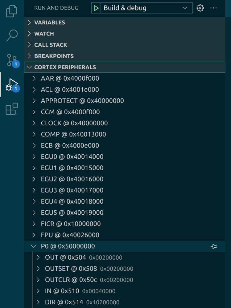
Note that in debug view in VSCode, you can conveniently see this information in the CORTEX Peripherals pane:

Setting the Pin Direction to Output#
OK, now it’s time to actually change some of these memory-mapped configuration registers. We’ll use the load-twiddle-store pattern.
The top-left LED is connected to Row 1 (P0.21) and Column 1 (P0.28). Let’s start by setting P0.21 (Row 1) to OUTPUT, that means setting a particular bit in the P0 DIR register to 1. We’ll need to follow these steps:
-
load: load the P0 base address into a register, then do an “offset”
ldrwith theDIRoffset to read the current state of theP0 DIRregister into a CPU register -
twiddle: use bitwise operations to set bit 21 (counting from the right) of
P0 DIRto 1 while leaving the other bits unchanged -
store: write the new
P0 DIRvalue back to the memory address you read it from earlier
When we talk about setting a bit, that means that it should be equal to 1,
and clearing a bit means it should be equal to 0. In addition, when performing
operations on a single bit, only the bit you are intending to change should change,
the rest should remain in their previous state.
So what does the code to perform these load-twiddle-store steps look like?
@ load r1 with the base address of P0
ldr r1, =0x50000000

@ load r2 with the value of P0 DIR
@ (note the 0x514 offset from the P0 base address)
ldr r2, [r1, 0x514]

@ set bit 21 by doing a logical or with 0b1 left-shifted by 21
@ think: why does this work?
mov r3, 0b1
lsl r3, r3, #21
orr r2, r2, r3

@ store the modified result back into P0 DIR
str r2, [r1, 0x514]
Why is the load part of this process necessary? Why can’t you
just store a single bit into the P0 DIR register and be done with it?
We have set one pin (P0.21) to output, but the LED is also connected to (P0.28) and that needs to be set to output as well. Copy the above code into your program and modify it so that you are setting bit 21 and 28 to output.
Setting a Pin’s Output to “High”#
Now that the output direction is set correctly for P0.21 and P0.28, we can actually turn on the LED!
A bit more background: LEDs, like most electrical components have two connections, you might have heard them being called “positive” and “negative” or “+” and “-“. On the microbit, each LED has it’s positive side connected to a ROW pin and it’s negative side connected to a COLUMN pin (how do we know? The circuit is in the microbit schematics :-D).
This means that to turn an LED on, we have to set the corresponding ROW pin to “high” (binary 1), and the COLUMN pin to “low” (binary 0) to create a circuit so that current flows through the LED and it lights up!
COMP2300 is where coding meets the “real” world of electronics, circuits and voltages and the language can be a bit confusing for non-electrical-engineers. While we have “+” and “-“ terminals on a battery or an LED, GPIO pins are always set to either “high” or “low” voltage.
Time to light it up! Copy-paste a second copy of the
load-twiddle-store code above. This time, you need to change the P0 OUT
register at offset 0x504 so that bit 21 is binary 1, that is, ROW 1 is set to
“high”. You shouldn’t need to change COLUMN 1 to “low”, but you can if you want
to.
Following the steps above, write a program which turns on the top left LED on your
microbit.
Copy the code into tasks/task-4.S. Commit and push your changes with the message “completed task 4”.
There are a few fiddly things which can go wrong here. If your LED isn’t coming on, talk with your neighbour/tutor about your program. Have you accidentally set the wrong bit (remember that the ports and bits are 0-indexed, so the rightmost bit is bit 0, not bit 1). Are you reading the existing register value correctly? Are you turning the bit on correctly? Are you writing it back to the right memory address? Step through the program with your partner to see what might be going wrong.
Task 5: Blinky#
In this exercise you’ll add a simple loop into your program to blink one of the
LEDs on and off. You can write some delay code to do this. The idea is that
in between turning your LED on and off your microbit should enter a loop that
will take a long time to exit.
You know how to turn an LED on. You probably can work out how to turn it off. If you set your code to turn the LED on and then off straight away (no delay) will you notice the change? If you blink an LED very quickly like this, will it look like it’s on, or will it look like it’s off? Try it with your neighbour and find out.
Now that you have tried turning the LED on and off immediately, it’s time to
introduce a delay. Create a delay label in between the LED turning on and
off. The idea will be to create a loop of some sort to return to that delay
label. There are a bunch of ways to do this, but one way is to
- set a register to a big number
- subtract 1 from this register,
- if the value isn’t zero then goto step 2, else exit the loop.
Modify your program so that after the initial setup code, there is a loop which turns the LED on, delays a little while, turns it back off, delays a little again, then branches back to the top of the loop. Once you’ve done that, you should be able to blink the LEDs on your board to your heart’s content.
Copy the code into tasks/task-5.S. Commit and push your changes with the message “completed task 5”.
Task 6: Boxy#
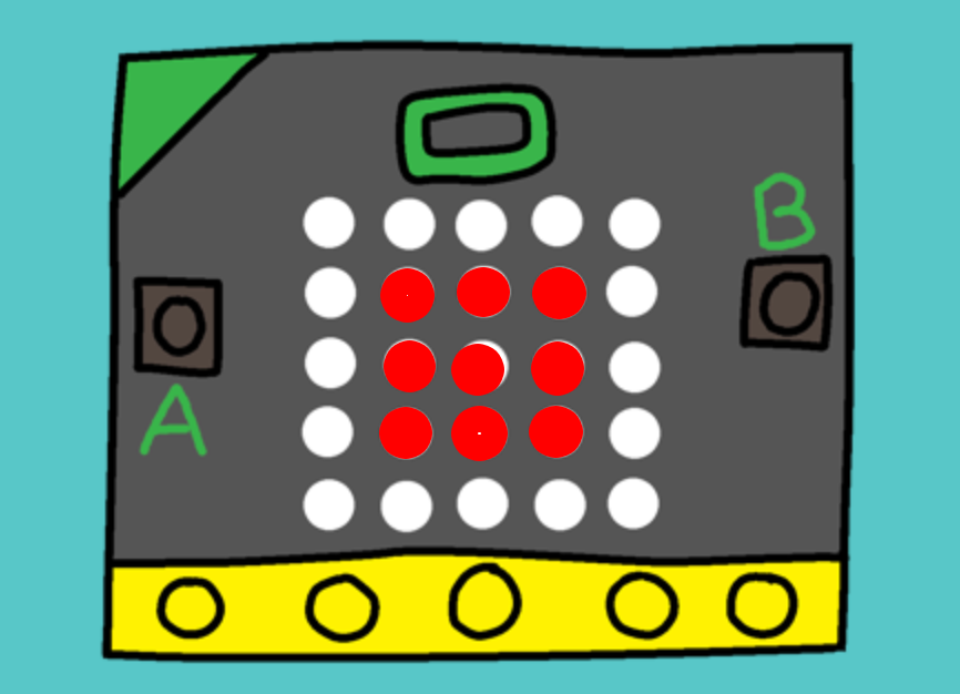
No hand holding here, for this exercise you need to light up and blink the 9 LEDS in the center of the microbit 5x5 grid.

Copy the code into tasks/task-6.S. Commit and push your changes with the message “completed task 6”.
What if I asked you to only light up the 8 LEDs in the center, with the middle-most LED off, could you do it? Remember how the circuits for the LEDs work; is it possible?
Wow! You made it to the end of the lab! You should be able to bathe in the warm light of glowing red LED(s).
Extra Tasks#
Any LED#
Create a program that can turn any single LED on the microbit on or off. Are there any limitations about what LEDs could be turned on at the same time?
Glowy#
Turning things on and of with a fixed delay is cool, but you can achieve more subtle effects with the LED using pulse-width modulation (PWM). The basic idea is this: if you want the LED to glow brightly, then (in a loop) leave it on for a long time, and turn it off for a short time. If you want it to glow dimly, do the opposite. Using this technique, can you make the LED look like it’s breathing?
Morse Code#
Can you store some data in your program somewhere to blink a more complex pattern—can you program your microbit to blink in Morse Code?
Immediate Values in ARM#
If you’re interested in how exactly the ARM instruction defines which constants can be stored inside a 32-bit instruction, then here’s an interesting blog post. Recall we use the Thumb-2 instruction set, so it’s not exactly the same on the microbit (see section A5.3.2 in the reference manual for how they work on the microbit).
Instead, you can play with the following widget to see how our board encodes a shift. The top input is the 12-bit encoded value. The second input is the 32-bit expanded output. Below this, the longer table is the binary representation of the output. An orange colour represents one of the 4 “special” shifts, while blue means it is a regular shifted byte. Similarly, the shorter table shows the parts of the encoded input, with the shift in purple and the data in green. Note how bit 7 of the encoded input is conditionally part of the shift or data, depending on bits 10 and 11. Each bit in the binary table can also be toggled by clicking it.