In this assessment you are going to complete a number of Digital files to a required spec, much like what you have already been doing in the labs.
To complete this assessment you should have completed the week 1, week 2 and week 3 labs as well as watched the week 1, week 2 and week 3 lectures.
This assessment task will be an opportunity for you to receive feedback on your progress in this course prior to the semester 1 census date (31st March).
Outline#
- Deadline: 10 March 2025, 11:59 pm
- Assessment template: link
- Specification: keep reading 🙂
- Weighting: 5%
- Marked out of: _ / 5
Time Until Deadline (10 March 2025, 11:59 pm): Deadline has passed!
Rules and Policies#
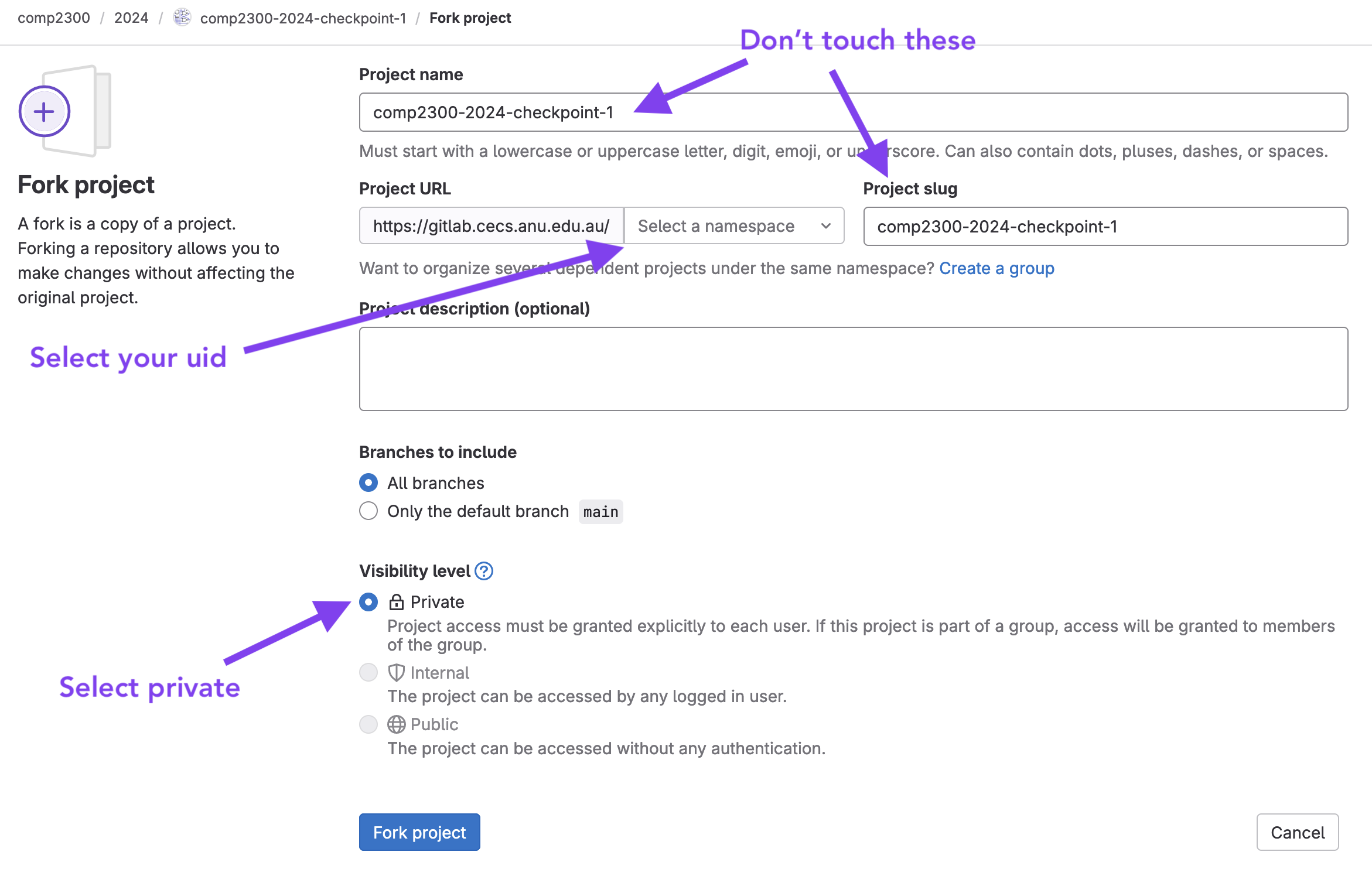
- this is an individual assessment task, ensure you fork your repo as private
- you may re-use designs / files from your labs
- it is your responsibility to ensure any additional files are included in the repo and pushed to gitlab correctly
- your main solution still needs to be in the provided files
- all submitted files should abide by the style guidelines
- late submission is not permitted without an extension
Disallowed Components#
The components you are allowed to use for each exercise differs, and is specified fully below. The following is a list of components you are not allowed to use in completing any of the following exercises:
- Lookup Table/LUT
- Counter
- Counter with preset
- Negation (Components > Arithmetic > Negation)
- VHDL / Verilog / Anything outside of Digital
- Priority Encoder
- Anything under the “IO > Displays”, “IO > Mechanical” and “IO > Peripherals” menu. E.g. MIDI keyboards.
You also should not add additional input or output components (“IO > Input” and “IO > Output”) to the template files. You also should not modify their names or bit counts.
Specification#
Exercise 1: MUX Negator#
We recommend completing lab 1 before attempting this exercise.
For the first exercise, your goal is to design a circuit that:
- Takes in 4, 4-bit inputs (
A,B,C,D) - Selects the appropriate input based on a 2-bit selector (
S) - Conditionally negates (inverts) the 4-bit input based on a 1-bit input (
T) - Outputs the 4-bit value (
Q).
When implementing this circuit, you should use the in-built multiplexer component where needed.
This leaves us with the following output table:
| A | B | C | D | S | T | Q |
|---|---|---|---|---|---|---|
| a | b | c | d | 0b00 |
0b0 |
a |
| a | b | c | d | 0b00 |
0b1 |
~a |
| a | b | c | d | 0b01 |
0b0 |
b |
| a | b | c | d | 0b01 |
0b1 |
~b |
| a | b | c | d | 0b10 |
0b0 |
c |
| a | b | c | d | 0b10 |
0b1 |
~c |
| a | b | c | d | 0b11 |
0b0 |
d |
| a | b | c | d | 0b11 |
0b1 |
~d |
Where a, b, c, d are some 4 bit binary value, and ~a, ~b, ~c, and ~d are their logical negation (inverse).
Eg: a = 0b1011, ~a = 0b0100.
Complete the ex1.dig file according to the above specification.
Exercise 2: Extended ALU#
We recommend completing lab 2 before attempting this exercise.
In this exercise, you will extend and modify the ALU you created in lab 2.
Your task is to design a circuit that:
- Takes in 2, 16-bit inputs (
A,B) - Performs the appropriate operation on the inputs based on a 3-bit selector (
ALUOP) - Outputs the 16-bit result (
RESULT) - Sets flags as necessary (
FLAG)
Here is the table for the ALUOP selector:
| ALUOP | Operation |
|---|---|
0b000 |
ADD |
0b001 |
SUB |
0b010 |
NAND |
0b011 |
NOR |
0b100 |
AND |
0b101 |
ORR |
0b110 |
XOR |
0b111 |
NOT |
When implementing the unary “NOT” you should set RESULT to be the bitwise
negation of A. The value of B does not matter in this case.
For a description of how to set the flags, please refer to the lab 2 page.
A quick summary:
Zero: set if the result is all0sNegative: set if the result is negative for 16-bit two’s complement (most significant bit is1)Carry: set if the addition of 2 inputs is larger than what can be represented in 16 bits0for non-arithmetic operations (carry not set)
- o
Verflow: set if the sign bit (most significant bit) of 2 inputs is the same, but the result after an addition is different from the inputs’ sign bit0for non-arithmetic operations (overflow not set)
We define an arithmetic operation as the ADD and SUB operations. All
others are non-arithmetic operations.
For the above definitions, we consider subtraction to also be performed as an addition, read here if you are confused as to why.
Complete ex2.dig to the above specification.
Disallowed Components#
The following components are disallowed for this exercise (in addition to those listed above):
- Subtract
- Comparator
- Bit Counter
- Registers, Flip-Flops, Latches and all Memory components.
- If you’re unsure how you can implement subtraction without using the “subtract” component, see the relevant section of lab 2.
- If you’re unsure how you can calculate the
Zflag without using the comparator or bit counter, follow the advice in the hint box from this section of lab 2.
Exercise 3: Register Counter#
We recommend completing Lab 3 prior to attempting this exercise.
For the final exercise, you will combine registers and a counter circuit to build a register counter.
Your task is to design a circuit that:
- Contains four 16-bit registers R0, R1, R2 and R3
- Responds to the rising-edge of a clock line (
CLK) - Allows the value of a register to be set based on a 16-bit input (
IN). - Performs arithmetic and register modification operations based on a 2-bit selector
(
OP), writing the result to one of the four registers R0-R3. The register to write to is determined by the current value ofRd, whereRd = 0writes the result to R0, andRd = 3writes the result to R3. The value ofRdis an additional piece of state that needs to be maintained in your circuit. - Allows the destination register (Rd) of these operations to be updated using
the value of
DSTwhen a specific “Update Rd” operation is performed. - Maintains register state, and the current set
Rdthroughout.
The table for the OP selector is as follows
| OP | Operation | Explanation |
|---|---|---|
0b00 |
Rd := Rd + 1 |
Increments Rd |
0b01 |
Rd := Rd - 1 |
Decrements Rd |
0b10 |
Rd := IN |
Sets Rd to be the value of IN |
0b11 |
d = DST |
Sets the “destination register” for subsequent operations. |
You have been provided registers R0-R3 in the ex3.dig file already. You should not delete or rename these registers.
The registers are also set as measurement values, which is critical to the tests working properly; make sure if
you end up deleting them accidentally that you set this option again. Where this option is located is described
in Lab 4 Exercise 1.
You will need to determine an appropriate way of storing which register is the current destination register and add this to your circuit yourself1.
For example, the following table shows how the registers change over time with the CLK line and OP code:
| CLK | OP | IN | DST | R0 | R1 | R2 | R3 | Explanation |
|---|---|---|---|---|---|---|---|---|
0 |
x |
x |
x |
0 |
0 |
0 |
0 |
Initial State |
C |
0b00 |
x |
x |
1 |
0 |
0 |
0 |
R0 := R0 + 1, as OP=0b00 (increment). |
C |
0b00 |
x |
x |
2 |
0 |
0 |
0 |
R0 := R0 + 1, as OP=0b00 (increment). |
C |
0b11 |
x |
1 |
2 |
0 |
0 |
0 |
Rd is updated to be 1. Future operations will operate on R1. |
C |
0b00 |
x |
x |
2 |
1 |
0 |
0 |
R1 := R1 + 1, as OP=0b00 (increment). |
C |
0b10 |
9 |
x |
2 |
9 |
0 |
0 |
R1 := 9, as OP=0b10 (set). |
C |
0b11 |
x |
3 |
2 |
9 |
0 |
0 |
Rd is updated to be 3. Future operations will operate on R3. |
C |
0b01 |
x |
x |
2 |
9 |
0 |
0xFFFF |
R3 := R3 - 1, as OP=0b01. |
Notes:
- X is the same as Digital tests where it doesn’t matter what value it is at this time.
Calso behaves like it does in Digital tests, see here for more info.- The initial destination register will be
0. This means any operations that occur before updatingRdwill write the results toR0. - You should implement incrementing and decrementing with only a single adder, instead of using separate subtracter and adder components.
Complete ex3.dig to the above specification.
Disallowed Components#
The following components are disallowed for this exercise (in addition to those listed above):
- Subtract
- Comparator
- RAM
- If you’re stuck trying to figure out how to only write to the relevant destination register in each clock cycle, try looking at Digital’s demultiplexer component (or complete the register file exercise from lab 3).
Marking Criteria#
This checkpoint will be entirely automarked, based on the results of:
- The CI tests (3 marks)
- Additional test cases that are run on your submission after the deadline. (2 marks)
The total marks are distributed between the three exercises as follows:
- Exercise 1 (1 mark)
- Exercise 2 (1.5 marks)
- Exercise 3 (2.5 marks)
Item 1 will be evaluated primarily through the results of tests identical to those provided in the template files, alongside additional tests in the CI to check whether you have followed the specification of allowed and disallowed components.
Item 2 will be evaluated through additional tests cases not provided you after the due date. These will test conformance to other parts of this specification, which can include (but is not limited to) additional edge cases and the efficiency of your circuits.
Incorrectly filling out your statement of originality may result in a mark of 0, regardless of the results of the other tests.
Style & Efficiency#
As the checkpoint will be auto-marked your conformance to the style guide will not be directly assessed. We recommend following the style guide regardless, as it will make understanding the circuit you design easier for you. It is also good practice for your first assignment which will include marks for style.
As mentioned in the marking section above, you will be marked on “efficiency” of your circuits. This doesn’t mean hyper-optimising your circuits to use as few components as possible, but this does include:
- Using a single
N-bit gate rather thanNseparate 1-bit gates where appropriate. In the following example, using a single 2-bitANDgate functions identically without taking up as much space. This is especially important for any adder components you use for e.g. exercise
2 and 3.
This is especially important for any adder components you use for e.g. exercise
2 and 3. - Only including one adder component to implement both addition and subtraction in exercises 2 and 3. You should also use the built-in adder, rather than one you created in lab 2.
- Not including unneeded registers in exercise 3.
- Using multiplexers with redundant cases. For example, if you only need to select between 4 different inputs you should not use an 8-to-1 multiplexer.
- Using multiplexers with only/mostly constant components where a logic gate
would suffice. For example:

Submission#
Submission is through GitLab, the most recently pushed commit of your fork of the assessment template before the deadline is taken to be your assessment submission.
Getting Started#
- read this assessment page completely
- fork and clone the assessment template
- ensure you fork your project as private
- do NOT change the name or path of the repo, or it may get missed by our software
- work on each task, testing, committing and pushing as you go
- make a mistake or get stuck, then ask a good question on the course forum.
Completion Checklist#
- you have completed the circuits in the files provided and have not renamed or moved them
- you have checked that you haven’t used any of the components listed above
- you have run your files local test(s) and they pass successfully
- you have laid out your circuits using good practice
- you have saved, committed and pushed your Digital files to gitlab
- you have filled out, committed, and pushed your statement of originality
- you have checked the gitlab ci tests and they are passing
- you have checked the pdf artifact on gitlab to ensure it is correct
Gitlab CI and Artifacts#
For this assignment, your mark is determined using the tests on gitlab. This is the CI that you may have already been seeing in the labs, however now it isn’t just for your benefit, so it’s important that you understand and check it.
The correctness of your implementations will be marked based on passing the tests for each one of the
exN.dig files. These tests will be similar to the ones that are
already present in the files, so if your digital files are testing okay locally, then they should also be
passing in the CI. However, it is best to make sure that this is the case by going to the gitlab website to
make sure the CI is passing as you’d expect.
To view the CI pipeline for your repo, click on the little icon to the right of your most recent commit.
![]()
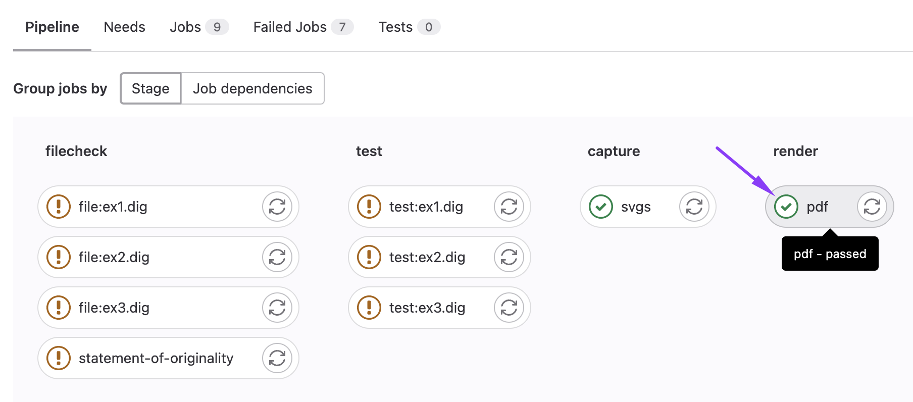
Then you’ll be presented with a list of the jobs, you’ll want to make sure that the jobs are passing once you’ve completed the corresponding task.
Filecheck stages ensure that the file exists and has been updated from the default. Test stages run the submitted files against our tests to measure correctness.
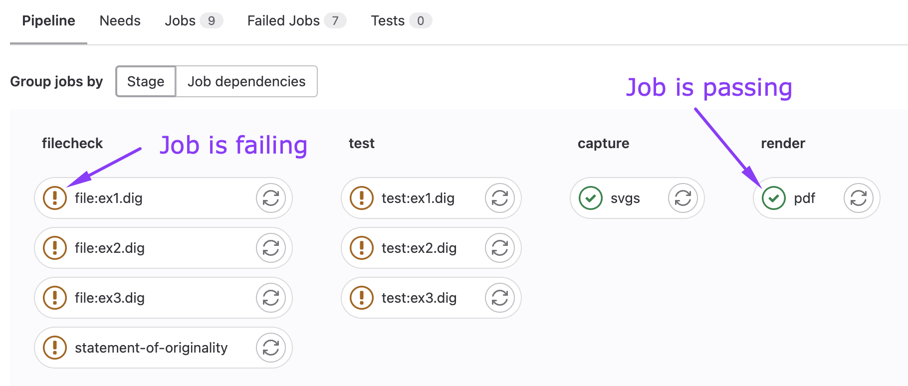
Alongside these functionality tests, there are a number of “validate” jobs that
check you haven’t used any disallowed components. Make sure your submission
passes both the test:exN.dig and validate:exN.dig jobs, as submissions that
utilize disallowed components will be penalized.
PDF Artifact#
Your repo will be packaged into a pdf for marking purposes. As such it is important that you see what the result
of the pdf job is and make sure the output makes sense.
It will:
- take your name and uid from the
statement-of-originality.md - take images from your
exN.digfiles - take test results similar to those in the
exN.digfiles - take references from the
statement-of-originality.md
To view the pdf, first click the ci icon on your most recent commit (as above), then click on the
pdf job.
Then, you’ll be taken to the job page, where you should see a “Job Artifacts” section, click on the Browse button.
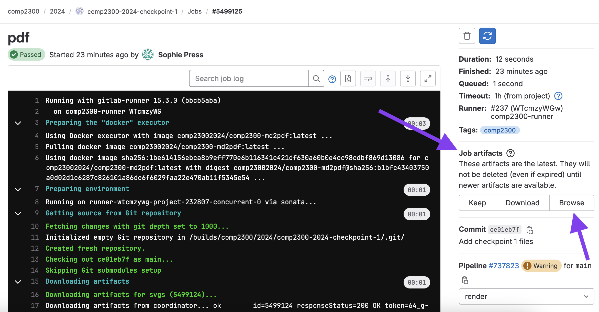
This will allow you to preview your pdf. Which should look something like this.
There is more general info about gitlab ci here.
FAQ#
My circuits don’t work, can I email you for help?#
Sorry, you won’t get help over email or Teams. We provide a course forum which is the only way we are able to help.
Forum posts related to your assessment submission must be “private” (as for any individual assessment task).
Why are my CI jobs failing?#
You can click on a failing job to read the output of the job. This will tell you why the job failed. For example:


In this specific case, we can see the job failed due to the statement of originality file being incorrectly filled out.
It’s [5 minutes, 60 minutes, 12 hours] before the deadline and my CI Jobs aren’t finishing!#
Unfortunately on the day that an assessment is due, when many students are pushing updates at once, the CI servers can’t keep up. You may not see your CI jobs finish before the deadline. You will just have to manually check that your files have been submitted correctly and that you are passing tests locally.
The best way to avoid this issue is to start early and finish early 😇
If there’s any issues with your git repository after the deadline. Please let us know (after the deadline) through a private forum post and there may be something we can do.
How do I know my assessment has been submitted?#
If:
- the files in your fork of the assessment are correct (i.e., the files you intend to submit) when checking on the gitlab website
- the time is before the deadline
then your assessment has been submitted (well done!).
Please don’t ask us to “check”, we would be just doing exactly the same thing as the above steps which you can do yourself.
Will I get marks for passing just the “Validate” tests?#
No. The validation tests on the CI check that you haven’t used any disallowed components in implementing your circuit. You need to pass both the tests for functionality and the validate tests to achieve marks in an exercise.
Will I get partial marks for passing the tests when I’ve used disallowed components?#
This depends on the specific exercise and the number/severity of disallowed components used. Most likely not.
Will I get partial marks for passing some test cases?#
The checkpoint will be automarked based on the pass/failure of individual jobs
in the CI as a whole, so if any cases fail you won’t be awarded the marks for
that exercise. Note that there is some leeway with exercise 2, as the tests
for the RESULT calculation is separated from the jobs that test the flags.
You can earn partial marks for this exercise if you complete the RESULT
calculation but not the flags, for example.
Can you give me a hint about the additional test cases?#
See the list in the Style & Efficiency section.
-
Try to be efficient about this as well — how many bits will you need to store the four possible values (0, 1, 2 or 3) that
Rdcan be set to? Would it make sense to use an additional 16-bit register for this?