This lab builds upon the content in Lab 2 and Lab 3. Furthermore, this week’s lab leads directly to the next lab. If you cannot finish this lab during your assigned session, you should make sure to finish it later. The content in this lab is critical.
The three labs 4, 5, and 6 all tie together, so consider them three parts of the same lab. You should move directly onto the next lab if you finish one early.
Outline#
In this week’s lab, you will:
- Learn to hook up the ALU and register file from previous labs to build a simpler version of the (final) CPU in the assignment.
- Learn how instructions are encoded and stored in memory.
- Learn about control signals and manually toggle the control lines to execute simple instructions by hand.
Preparation#
Before you attend this week’s lab make sure:
-
You have a working and tested the ALU from the ALU lab (week 3)
-
You have a working and tested register file from the register file lab (week 4)
Introduction#
Our goal in the first half of this course is to build a Central Processing Unit (CPU). We also call it the processor or the microprocessor. As discussed in the introductory lecture, the CPU is the heart of a computer system. Interestingly, in the previous labs, we have built two critical components of a modern CPU, the ALU and the register file. But we have built and tested these two components in isolation. In this lab, we will connect these parts together to form a rudimentary CPU. Doing this will help us understand how the processor (and a typical computer system) works as a whole.
Note that a CPU has three major components:
- Arithmetic and Logic Unit (ALU)
- Register File (RF)
- Control Unit
From time to time, we will also need to add other components (multiplexers and decoders) to glue everything together. We often refer to this extra logic as glue logic. The primary purpose of glue logic is to route signals to the correct components in the circuit. You will learn to add glue logic as you gain more practical experience hooking together the three components above.
Every computer system needs main memory to store the code and data for the applications we execute on the processor and the computer system. Main memory is not technically considered part of the CPU. On the other hand, no computer system can operate without one. Therefore, we will include main memory (or just memory) in the final design. We will then need to interface the CPU with memory.
The high level organization of a CPU (its microarchitecture) is graphically depicted in the form of a block diagram.
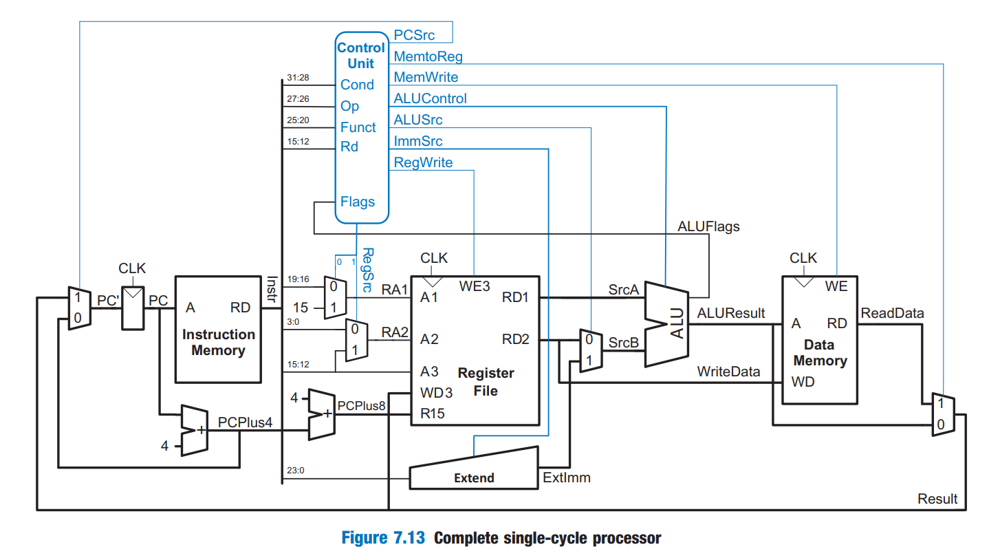 Textbook CPU microarchitecture (not the CPU we will build in the assignment)
(courtesy of Digital Design and Computer Architecture, Harris & Harris)
Textbook CPU microarchitecture (not the CPU we will build in the assignment)
(courtesy of Digital Design and Computer Architecture, Harris & Harris)
This high-level diagram splits the CPU into a few major components and demonstrates how they are linked together. We can see the register file and ALU that we built in previous labs, two memory units for code and data, and glue logic to tie the machine together. Once again, please remember that the CPU in the assignment is different from the one in the textbook.
Note in this diagram the control signals in blue. These blue signals are hooked to the various components of the CPU. They dictate what operation the ALU performs and which registers the register file reads from and writes to. We will manually control the blue (control) lines in this lab.
Background#
Computers (and CPUs) do not speak English. Therefore, to instruct a CPU to do something useful for us (e.g., add two numbers), we need to learn its language. The words in a computer’s language are instructions, and the computer’s vocabulary is the instruction set architecture. We often refer to a computer’s instruction set architecture as an ISA. Note that ISA is just a specification. It is the list of instructions a computer can perform and the format of specific instructions. These instructions are encoded in binary with 1’s and 0’s so the CPU can understand them. We build a CPU to adhere to a specific ISA. There are many popular ISAs in use today. For example, x86 and ARM are famous ISAs in the desktop and mobile markets, respectively.
All programs running on a computer use the same instruction set. All complex software applications, such as Word and Spotify, are broken down into a sequence of simple instructions.
Remember never to confuse your CPU with the use of words outside its vocabulary.
Computer instructions indicate both the operation to perform and the operands to use. The operands may come from memory, from registers, or from the instruction itself.
A CPU executes a complex application with a fetch-decode-execute cycle. Instructions initially reside in the main memory. The CPU fetches an instruction from memory, decodes the instruction, and then executes it. This cycle repeats until the CPU runs out of instructions to perform. An instruction is nothing but a sequence of bytes. All ISAs include instructions to load bytes from memory and store bytes to memory.
Next week, we will build a control unit that will allow the CPU to read an instruction from memory, decode it, and then execute the instruction by using the control lines to automatically activate various parts of the CPU. For the moment, we will subsume the working of the control unit and toggle these lines manually. (Think of this phenomenon as hijacking the CPU’s control unit and making it do things manually.)
Exercise 0: Prerequisite Files#
You will not be able to start this lab without first completing the register file and ALU from previous labs.
Copy the files alu.dig from Lab 2
and reg_file.dig from Lab 3
into the folder for this lab (lab-04).
Ensure they pass their respective tests and meet the specification below.
ALU Specification#
You only need the Z and N flags working for this lab. Do not waste time
implementing the other flags (C and V). However, you will need all flags
for the assignment.
The ALU should have the following input ports
ALUOP(2-bits) to select which operation to performA(16 bits) The first operand (input) to the ALUB(16 bits) The second operand (input) to the ALU
The meaning of OP is as follows:
ALUOP |
Mnemonic | Meaning | ALU Behaviour |
|---|---|---|---|
00 |
XOR |
Bitwise XOR | RESULT = A ^ B |
01 |
AND |
Bitwise AND | RESULT = A & B |
10 |
ADD |
Addition | RESULT = A + B |
11 |
SUB |
Subtraction | RESULT = A - B |
and output ports
RESULT(16-bits) The result of the operation (output)FLAG(4-bits) The status flags generated by the result of the operation, arranged as follows:
| Bit Index | Flag | Meaning | Behaviour |
|---|---|---|---|
| 0 | Z | Zero | RESULT is zero |
| 1 | C | Carry | Carry was generated* |
| 2 | V | Overflow | Overflow was generated* |
| 3 | N | Negative | RESULT is negative (signed) |
(* see lab 2 for how each status bit is defined.)
Register File Specification#
The register file should have ports
RS1(3-bits): Read Select 1, Chooses which register to send to the first output OUT1.RS2(3-bits): Read Select 2, Chooses which register to send to the second output OUT2.WS(3-bits): Write Select, Chooses which register to write to on the next positive clock edge.WE(1-bit): Write Enable, If HIGH, the register specified by WS will be written to on the next positive clock edge. If LOW, the registers are unaffected.IN(16-bits) the data to be stored.OUT1(16-bits) the value stored in the first register selected.OUT2(16-bits) the value stored in the second register selected.CLK(1-bit) clock line.
There are 3-bits to specify a register, encoded as follows:
| Code | Mnemonic | Meaning | Behaviour |
|---|---|---|---|
| 000 | RZ |
Zero Register | Always read zero, writes have no effect. |
| 001 | R1 |
Register 1 | General purpose register. |
| 010 | R2 |
Register 2 | General purpose register. |
| 011 | R3 |
Register 3 | General purpose register. |
| 100 | R4 |
Register 4 | General purpose register. |
| 101 | - | undefined | Read and write is undefined. |
| 110 | - | undefined | Read and write is undefined. |
| 111 | - | undefined | Read and write is undefined. |
(see lab 3 for more details.)
Why do we waste a register code on a dummy do-nothing register? If you cannot see why, you will find out soon.
Exercise 1: Building a Computer Calculator#
We first consider a greatly simplified version of a computer where the only components are the ALU and register file and for which we control the control signals manually. Consider the following block diagram:
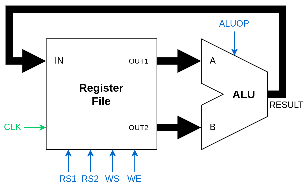 A regfile interfaced with an ALU, with manual control lines.
Using calc.dig as a template, build a circuit according to the block diagram
presented above. You should have the following control lines:
ALUOP(2-bits): ALU Operation, tells the ALU which operation to performRS1(3-bits): Read Select 1, chooses which register to send to the first output.RS2(3-bits): Read Select 2, chooses which register to send to the second output.WS(3-bits): Write Select, chooses which register to write to on the next positive clock edgeWE(1-bit): Write Enable, if HIGH, the register specified byWSwill be written to on the next positive clock edge.
You might find that the custom components are too narrow, and the labels for the pins collide. To fix this problem, open the custom circuit, navigate Edit -> Circuit Specific Settings and adjust the Width as appropriate (somewhere around 5-8 is probably ideal).
If you are interested in your custom circuits having a more
interesting shape than a boring rectangle,
the go under Edit -> Circuit Specific Settings and Advanced, and you can
export a template as an .svg file (which is a rectangle with
the input/output pins representing that custom circuit). You can
then edit the .svg file (using Inkscape or some other image
editing program) and rearrange the order of the pins, or even make the
shape of the circuit something other than a rectangle (like the trapezoidal
shape usually used to represent an ALU).
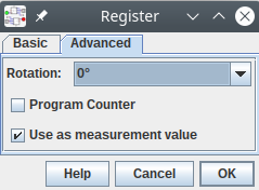
It can be hard to keep track of the state of components that are abstracted away inside other components. To help with this you can:
- right-click on a register
- ensure that the register has a
Label - click on the Advanced tab and check Use as a measurement value
- press Ok
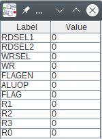
During simulation, you can then open Simulation -> Show measurement value table (or press F6) which will show the value of all inputs and outputs in the circuit, as well as any other values you have designated as measurement values. You can also edit the value stored inside a component using the table directly.
- Right-click on the register file and click Open Circuit. Mark all registers in the register file as measurement values. Save and close the register file.
- Back in the
calc.dig, add a probe (Components -> IO -> Probe), and label the probeRESULT. - Connect the probe to the
RESULTport on the ALU. - Right-click on the probe and label it
Now that we have our calculator built, we can make it perform some operations.
You may find this tool that will convert between decimal, binary and hexadecimal representations of numbers useful when completing this and future exercises.
| Decimal | |
| Hex | |
| Binary |
Start the simulation and open the measurement table (Simulation -> Show measurement value table), and store the values R1 = 1, R2 = 3, R3 = 0xF.
Using only the control lines and toggling the clock,
perform the following operations
- Do nothing (none of the registers should change when the clock is toggled).
- Set
R4to0x10 - Set
R4to0xC - Set
R4to0xFFFF(Hint: Recall how negative numbers are encoded, and thatRZ(register code000) is always zero).
Note down what you had to do for each case because you will need it to write a test later.
You can toggle the clock line by pressing c.
The sequence of control line toggles required to achieve these operations is essentially what the control unit does: It takes as input the encoding of an instruction to execute, and then dictates to the computer how to perform that operation. Here, we are performing the job of the control unit manually.
We can also test sequential circuits. Since sequential circuits depend on the current input as well as past inputs, it is not possible to enumerate all possible inputs as we did for combinational circuits. Tests for sequential circuits look more like a computer program, where we can specify the inputs, toggle the clock line, and then check if the new outputs match what we expect.
If a C is encountered in a
test, all the other values are set as the test describes, and then the
signal associated with C is then toggled (switched from LOW to HIGH, and then
back from HIGH to LOW). The test is then checked against for correctness.
This means that we can write a test where we can set some control
signals, toggle the clock line, and then check the expected result.
We can also ask the test to initialise registers (or anything else with state)
by using the init keyword, and specifying both the label of the register, and
the value we would like to set it to. For example, if we wanted to test
that adding R1 to R2 and storing in R4 means that R4 = 4 afterwards,
we could write the following test:
# Testing R4 := R1 + R2
# Assuming R1 = 1 and R2 = 3
# op = 2 (addition)
# RS1 = 1 (R1)
# RS2 = 2 (R2)
# WS  = 4 (R4)
# WE  = 1 (enable writing to register)

CLK OP RS1 RS2 WS WE    R1 R2 R3 R4

init R1=1;
init R2=3;
init R3=0xF;

0   0   0   0   0  0    1  3  0xF x    #R1 = 1, R2 = 3, R3 = 0xF, R4 uninitalised
C   2   1   2   4  1    1  3  0xF 4    #R4 = 4, all other registers unchanged
Using the template given, replace the ? to create a test that automates
the operations you did in the previous exercise to set R4 to the required values
and then uncomment the test lines (remove the # at the beginning of the those lines).
If it took multiple operations to set one of the values, add extra lines
in between, and check the intermediate values are also correct.
Note that the CALC test will fail if you don’t have any uncommented lines in it, so
if it fails before you add anything, remove the # at the beginning of the first
and second lines.
# Testing the simple manual calculator
# CLK: Clock
# ALUOP: ALU opcode
# RS1: First operand
# RS2: Second operand
# RD: Destination register to write to
# WE: Write enable
# R0-R3: Registers

CLK ALUOP RS1 RS2 WS WE    R1 R2 R3 R4

init R1=1;
init R2=3;
init R3=0xF;

# 0   0    0   0   0  0      1  3  0xF 0       #ensure registers initalised correctly
# C   ?    ?   ?   ?  ?      1  3  0xF 0       #do nothing
# C   ?    ?   ?   ?  ?      x  x  x   0x10    #R4 = 0x10
# C   ?    ?   ?   ?  ?      x  x  x   0xC     #R4 = 0xC
# C   ?    ?   ?   ?  ?      x  x  x   0xFFFF  #R4 = 0xFFFF
Solution: Click here to see what the test case should look like.
CLK ALUOP RS1 RS2 WS WE  R1 R2 R3 R4

init R1=1;
init R2=3;
init R3=0xF;

0   0     0   0   0  0   1  3  0xF 0       #ensure registers initalised correctly
C   0     0   0   0  0   1  3  0xF 0       #do nothing
C   2     1   3   4  1   x  x  x   0x10    #R4 = 0x10   (R4 = R3 + R1)
C   3     3   2   4  1   x  x  x   0xC     #R4 = 0xC    (R4 = R3 - R2)
C   3     0   1   4  1   x  x  x   0xFFFF  #R4 = 0xFFFF (R4 = R0 - R1)
The ALU has also got a flag output that we’ve been ignoring for the moment. Let us add some status lights to each bit of the flag.

The flags in the 4-bit FLAG output from the ALU are arranged as follows.
- \(Z\) is the zero flag
- \(C\) is the carry flag
- \(V\) is the overflow flag
- \(N\) is the negative flag
Add some outputs Components -> IO -> Output to calc.dig that matches the provided block diagram.
Use the labels Z, C, V, N as appropriate.
Exercise 2: Load and Store#
We digress for a moment to look at how CPU-memory interaction works. As a start, we are going to use synchronous memory. The synchronous aspect means the exact moment in time when the data is stored in memory is controlled by the rising edge of a clock line.
Digital provides a pre-built module for memory that we will use here. The component is called RAM (Random Access Memory) because each (random) location can be accessed in the same amount of time. It is used as follows:
A: The address to where data should be stored.Din: The data to write to memory.D: The data to read from memory.C: Clockstr: If HIGH, the memory will store the dataDinat addressAon the next positive clock edge.ld: If HIGH, then the data stored at addressAis output onD. Else,Dis disconnected.
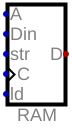
Find this component under Components -> Memory -> RAM -> RAM, separated Ports
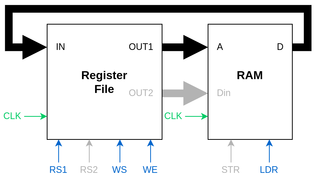
Now, consider the following block diagram, comprised of our register
file, and a memory block. We have the same control lines
as before, with the addition of
STR (1-bit) and LD (1-bit) that control the respective lines to memory.
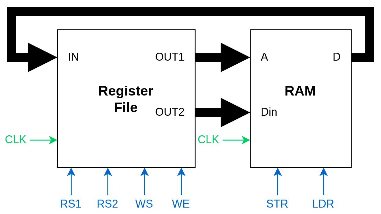
This circuit can perform one of two operations:
- Load: Loading data from memory to the register file.
- Store: Storing data from the register file to memory.
We can show how the data flows (and what control lines are active/in use) for a store/load below.
 Loading data from memory
 Storing data to memory
Using load_and_store.dig as a template, build a circuit according to the block diagram
presented. You should have the following control lines:
RS1(3-bits): Read Select 1, Chooses which register to send to the first output.RS2(3-bits): Read Select 2, Chooses which register to send to the second output.WS(3-bits): Write Select, Chooses which register to write to on the next positive clock edgeWE(1-bit): Write Enable, If HIGH, the register specified byWSwill be written to on the next positive clock edge.STR(1-bit): Store, tells the memory to store the data fed toDinat the address fed toA.LDR(1-bit): Load, tells the memory to load the data from addressAand output it toD. The registers inside the register file should be marked as measurement values.
In contrast with main memory (RAM), a storage device, such as a hard disk in your laptop, is not a random access device. The mechanical rotatory mechanism in disks means the time it takes to access an arbitrary byte is not the same and depends on the location of the byte on the disk.
Note that the RAM component has a 16-bit wide address bus and a 16-bit wide data bus which allows it to easily interface with our register file. Most computers today use either 32-bit or 64-bit wide addresses and an 8-bit wide data bus.
Do not delete the RAM component, as it’s preinitialised
with the following data (from ram.bin):
(all other memory slots contain zeros.)
In load_and_store.dig, start the simulation, and use the measurement table
to initialise R1 := 5, R2 := 3 and R3 := 1.
Right-click on the RAM module to view the contents.
Assume memory is initialised as per above, using the control signals:
- Load the data
0xAAAAfrom memory into registerR4. - Store the data
3into memory address0, overwriting the data0xAAAApresent. - Copy the data
0xBBBBfrom address1to address5.
Exercise 3: A Manual Computer#
We can now combine the two circuits together and extend our “calculator” from Exercise 1 to now have the ability to read and write to memory.
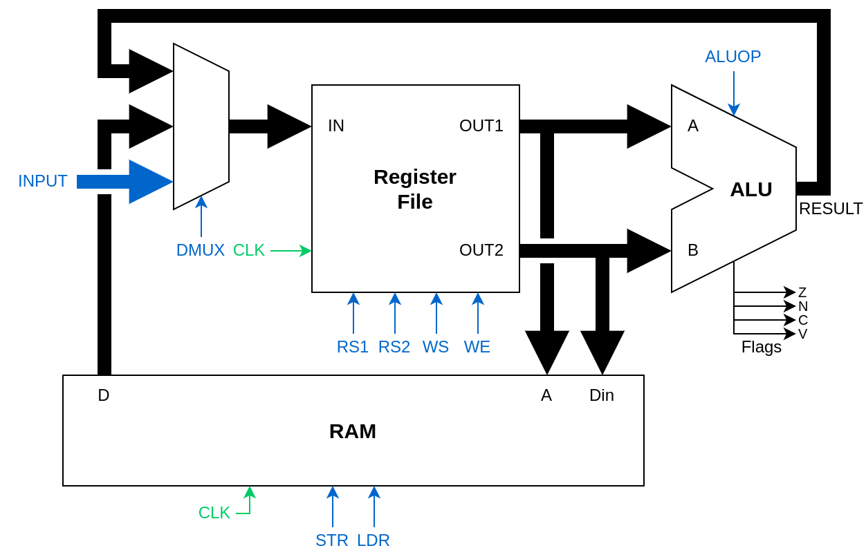 Register file interfaced with ALU and memory, with manual control lines.
We have also added an additional input so the user can directly write a value to a register (this will not remain in the final CPU).
Since there are now three devices that can write to the register file
(ALU, memory, user input), we need to add a multiplexer to choose
between them, and a corresponding control signal DMUX
that chooses which signal gets sent to the register file.
The signal sent to DMUX chooses a device as follows
| Signal | Device |
|---|---|
| 00 | - |
| 01 | ALU |
| 10 | Memory |
| 11 | User Input |
Using manual_cpu.dig as a template, build a circuit according to the block diagram
presented. You should have the following control lines:
ALUOP(2-bits): ALU Operation, tells the ALU which operation to perform.RS1(3-bits): Read Select 1, Chooses which register to send toOUT1, which connects toAon the ALU, as well as the address port on memory.RS2(3-bits): Read Select 2, Chooses which register to send toOUT2, which connects toBon the ALU, as well as the data port on memory.WS(3-bits): Write Select, Chooses which register to write to on the next positive clock edgeWE(1-bit): Write Enable, If HIGH, the register specified byWSwill be written to on the next positive clock edge.STR(1-bit): Store, tells the memory block to store data.LDR(1-bit): Load, tells the memory block to load data.DMUX(2-bits): Data Multiplexer, selects which device to write to the register file.IN(16-bits): User Input, allows the user to directly write to a register.
The registers inside the register file should be marked as measurement values.
Also included is a probe DATA so you can see the value coming out of the data multiplexer
that will be written to the register file on the next clock cycle.
Again, assume that memory is preinitialised as follows.
\[\begin{array}{cc} \text{Address} & \text{Data} \\ \hline \texttt{0000} & \texttt{0xAAAA} \\ \texttt{0001} & \texttt{0xBBBB} \\ \texttt{0002} & \texttt{0xCCCC} \\ \texttt{0003} & \texttt{0xDDDD} \\ \end{array}\]Using the control signals, perform the operation
mem[0x2] := mem[0x1] + mem[0x0]
That is, load from the first two slots, add the data from slot together, and store the result to the third slot. After doing so, the state of memory should be
\[\begin{array}{cc} \text{Address} & \text{Data} \\ \hline \texttt{0000} & \texttt{0xAAAA} \\ \texttt{0001} & \texttt{0xBBBB} \\ \texttt{0002} & \texttt{0x6665} \\ \texttt{0003} & \texttt{0xDDDD} \\ \end{array}\]We have also included a simple test that basically verifies the above, but it is good to do it manually by hand, so you have a clear idea about how all the control signals work.
Push all your work to GitLab, and move onto CPU, Part II