This lab is a sequel to CPU, Part I.
This lab has a very long preamble. You must read it all! There is information here to convey how the QuAC ISA is defined and how the CPU should behave for each instruction.
Outline#
In this week’s lab you will:
- Learn how instructions are encoded and stored in (main) memory.
- Understand what a control unit is, how it works, and build one in Digital.
- Integrate the control unit with other components to build a full CPU.
A subtle outcome of this lab is that you will learn to understand and graphically depict the high-level organization (microarchitecture) of a CPU.
An instruction set architecture (ISA) or simply architecture is the specification of a computer. The implementation of an ISA at the logic gate level is called its microarchitecture. A single ISA may have several distinct microarchitectures. We will introduce the hypothetical QuAC ISA in this lab. We will then help you build a microarchitecture for the QuAC ISA.
Preparation#
Before you attend this week’s lab, make sure
you have a working and tested manual CPU manual_cpu.dig, together
with its ALU alu.dig and register file reg_file.dig from
Lab 4.
Exercise 0: Documentation#
An engineer reads the documentation before undertaking construction! Indeed, it is vital to read the specification of the CPU before building it. Please find and read the QuAC ISA specification here. You can skim through the documentation initially, but read it in detail before starting the remaining exercises.
Introduction#
Last week we built a manual CPU, but manually toggling the control lines of a CPU is neither realistic nor fun. In reality, we would write a sequence of instructions for the CPU to perform and then sit back and watch the CPU control its own control lines.
To do so, we need
- A way to fetch instructions from memory. To aid instruction fetch from memory requires a special register called the Program Counter (
pc). - An agreed-upon encoding for instructions. This encoding is called the instruction format. There maybe more than one format in an ISA.
- A circuit for setting/resetting the control lines according to the instruction. We call this circuit the control unit.
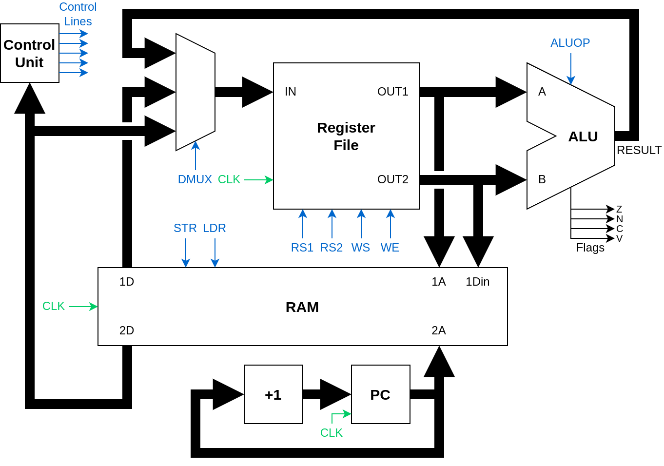
Consider the following block diagram, same as the manual computer, but with an additional register that indicates the current instruction to execute (called the program counter) and the control unit, which automatically toggles all control signals. We have upgraded the memory component to dual-port RAM that allows for simultaneous reads from two locations at once. This way, we can (1) fetch an instruction from memory and (2) load/store something to/from memory as required by the instruction. Remember that the CPU may need two interactions with memory to execute a single instruction.
Let us look at each of the three new aspects of our new computer built on top of the manual computer from the last lab.
Program Counter (pc)#
Let us first talk about fetching instructions from memory. We add an extra
16-bit register, the Program Counter (pc). The pc register holds the
address of the current instruction. We permanently connect the pc to one of the
address inputs of the memory component. We discuss the dual-port memory
component in detail later. For now, remember that we connect the pc to the
memory component’s second address input. After the CPU executes an
instruction, it increments the pc and gets ready to fetch the next
instruction from memory.
Encoding Instructions#
An ISA is a complete specification of each of the instructions we want our CPU to execute, how the instructions are encoded, and what each instruction does.
Humans instruct computers with instructions as shown here. The notation shown is known as the assembly language. Computers see instructions as a series of binary digits. This binary representation of instructions is called the machine language. A sequence of machine language instructions is called the machine code.
In the QuAC ISA, each instruction fits in exactly 16 bits. Note that not all the bits are allocated and many of the bits are reserved for future use.
There are two encodings for instructions, R-Format (Register Format) and I-Format (Immediate Format).
Register Operand Format (R-Format)#
| 15 | 14 | 13 | 12 | 11 | 10 | 9 | 8 | 7 | 6 | 5 | 4 | 3 | 2 | 1 | 0 |
|---|---|---|---|---|---|---|---|---|---|---|---|---|---|---|---|
op |
X |
rd |
0 | ra |
0 | rb |
|||||||||
Immediate Format (I-Format)#
| 15 | 14 | 13 | 12 | 11 | 10 | 9 | 8 | 7 | 6 | 5 | 4 | 3 | 2 | 1 | 0 |
|---|---|---|---|---|---|---|---|---|---|---|---|---|---|---|---|
op |
X |
rd |
imm8 |
||||||||||||
Both instruction encodings have the same meaning for the first (most significant) byte (8 bits) of the instruction.
| Name | Meaning | Description |
|---|---|---|
op |
Opcode | Specifies the operation to perform. |
X |
Future task | This will be used in a later exercise, but we ignore it for now. |
rd |
Destination / Data Register | (not str) Determines which register the result of this instruction is written to, or (for str) is used as the register containing the data to store to memory.1
|
R-Format only#
| Name | Meaning | Description |
|---|---|---|
| 0 | Literal zero | The value is always 0. |
ra |
First Operand / Address Register | The register used for the first operand in ALU instructions, or for the address in ldr and str. |
rb |
Second Operand Register | The register used for the second operand in ALU instructions. ldr and str set this to 0. |
I-Format Only#
| Name | Meaning | Description |
|---|---|---|
imm8 |
Immediate (8-bit) | An immediate, or constant, 8-bit value that is directly encoded into the instruction. |
Next, we will implement the following subset of the QuAC ISA. Specifically, we will focus on seven instructions:
- one immediate instruction (
movl), - two memory instructions (
ldr, andstr), and - four ALU instructions (
add,sub,and, andxor).
We will ignore several details regarding the program counter, flags, conditional execution, and the seth instruction for the moment.
| Syntax | Semantic | Machine Code |
| I-Format Instructions | ||
movl rd, imm8 |
rd ≔ #imm8 |
0000 0 <rd> <imm8> |
| R-Format Memory Instructions | ||
str rd, [ra] |
[ra] ≔ rd |
0100 0 <rd> 0 <ra> 0000 |
ldr rd, [ra] |
rd ≔ [ra] |
0101 0 <rd> 0 <ra> 0000 |
| R-Format ALU Instructions | ||
add rd, ra, rb |
rd ≔ ra + rb |
1000 0 <rd> 0 <ra> 0 <rb> |
sub rd, ra, rb |
rd ≔ ra - rb |
1001 0 <rd> 0 <ra> 0 <rb> |
and rd, ra, rb |
rd ≔ ra & rb |
1010 0 <rd> 0 <ra> 0 <rb> |
xor rd, ra, rb |
rd ≔ ra ^ rb |
1011 0 <rd> 0 <ra> 0 <rb> |
where
-
<rd>,<ra>,<rb>: 3-bit register codes, matching that of the register file from week 3. -
imm8An 8-bit constant in the range 0 to 255 inclusive. -
[ra]Represents the data at the memory address stored in register<ra>.
You should pay special attention to the [ra] notation. The specific register
<ra> is treated as a memory address when we place square brackets around the
register.
The register codes and their purpose is reproduced below. We will define some of the currently undefined register codes in future exercises.
| Code | Mnemonic | Meaning | Purpose |
|---|---|---|---|
| 000 | rz |
Zero Register | Always read zero, even after any write. |
| 001 | r1 |
Register 1 | General purpose register. |
| 010 | r2 |
Register 2 | General purpose register. |
| 011 | r3 |
Register 3 | General purpose register. |
| 100 | r4 |
Register 4 | General purpose register. |
| 101 | - | undefined | Read and write is undefined. |
| 110 | - | undefined | Read and write is undefined. |
| 111 | - | undefined | Read and write is undefined. |
A more verbose description of what each instruction does can be found here.
Control Unit#
Thirdly, we need to make some modifications to the CPU to allow the control lines to be set and reset from another circuit, a control unit, rather than controlling the lines manually. The control unit examines each instruction read from memory and generate control signals for ALUs, register files, and memory to make the rest of the CPU execute the instruction correctly. Note that the control unit can ignore the reserved bits in instructions.
We can divide the microarchitecture of QuAC ISA into two interacting parts: the datapath and the control unit. The datapath contains structures such as memories, ALU, registers, and multiplexers. The datapath operates on 16-bit data words. The control unit receives the instruction from the datapath and informs the datapath how to execute the instruction. Doing so requires the control unit to produce multiplexer select, register enable, ALU operation select, etc. This process is equivalent to decoding the meaning of an instruction. Therefore, the control unit must be made aware of the instruction encodings.
Dual-Port Memory#
Digital provides a pre-built component for dual-port memory that we will use here. It offers one port to read from and write to a memory address (first address or 1D) and a second port to only read from a memory address (second address or 2D). We will use the first address/data port for the CPU to load/store data to/from memory. We will use the second address/data port to fetch instructions from memory.
Inputs#
| Name | Description |
|---|---|
1A |
The address to store 1Din to, or read 1D from. |
1Din |
The data to store at the address 1A. |
2A |
The address to read 2D from. |
C |
Clock |
str |
If HIGH, the memory will store the data 1D at address 1A on the next positive clock edge. |
ld |
If HIGH, then the data stored at address 1A is output on 1D, and the data stored at 2A is output on 2D. |
Outputs#
| Name | Description |
|---|---|
1D |
The data read from address 1A. |
2D |
The data stored at address 2A. |
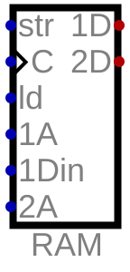 The dual port RAM component in Digital
Instruction Behaviour#
What follows is a description of how the CPU executes each instruction, together with a diagram that highlights how the data flows though the CPU, together with what the control unit is doing, and which control lines are used.
The program counter feeds into the second address port of memory for all instructions, and the control unit reads the instruction located at that memory address. The control unit decodes the instruction and generates several control signals to make the CPU (datapath) execute the specific instruction.
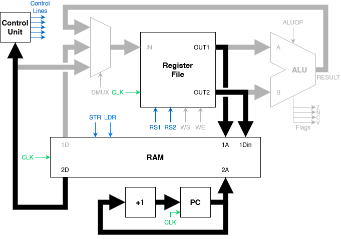
The add/sub/and/xor Instructions#
The opcode is of the form 10<aluop>. The last two bits of the
opcode, <aluop> indicate which ALU instruction should be
executed.
| Selector | Operation |
|---|---|
| 00 | ADD |
| 01 | SUB |
| 10 | AND |
| 11 | XOR |
The register file sends the registers specified by the register codes
<ra> and <rb> to the ALU, which performs the operation specified
by <aluop>. The result from the ALU is fed through the data multiplexer
(DMUX = 00) and the register file writes the result to
register <rd>.
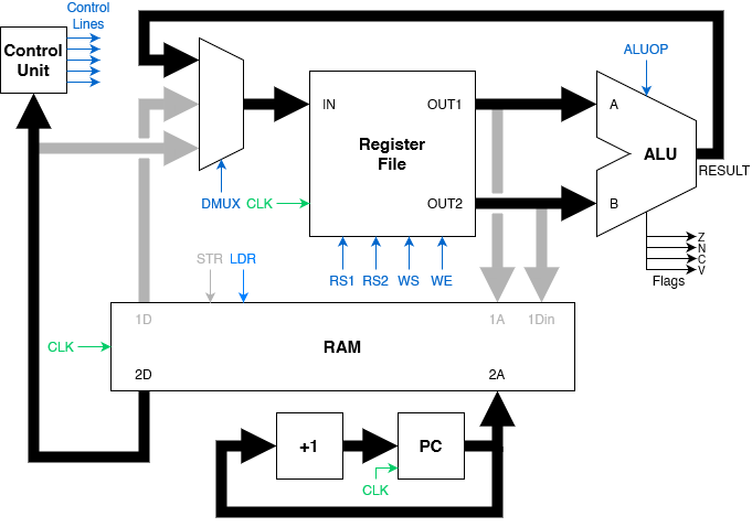
The ldr Instruction#
The register file outputs register <ra> to
the first address port on memory. The load signal on memory is set to high, and
the data from the first data out port on memory is fed through the data multiplexer
(DMUX = 01) and then the register file stores the data from memory
in the destination register <rd>.
 Loading data word from memory to register (ldr)
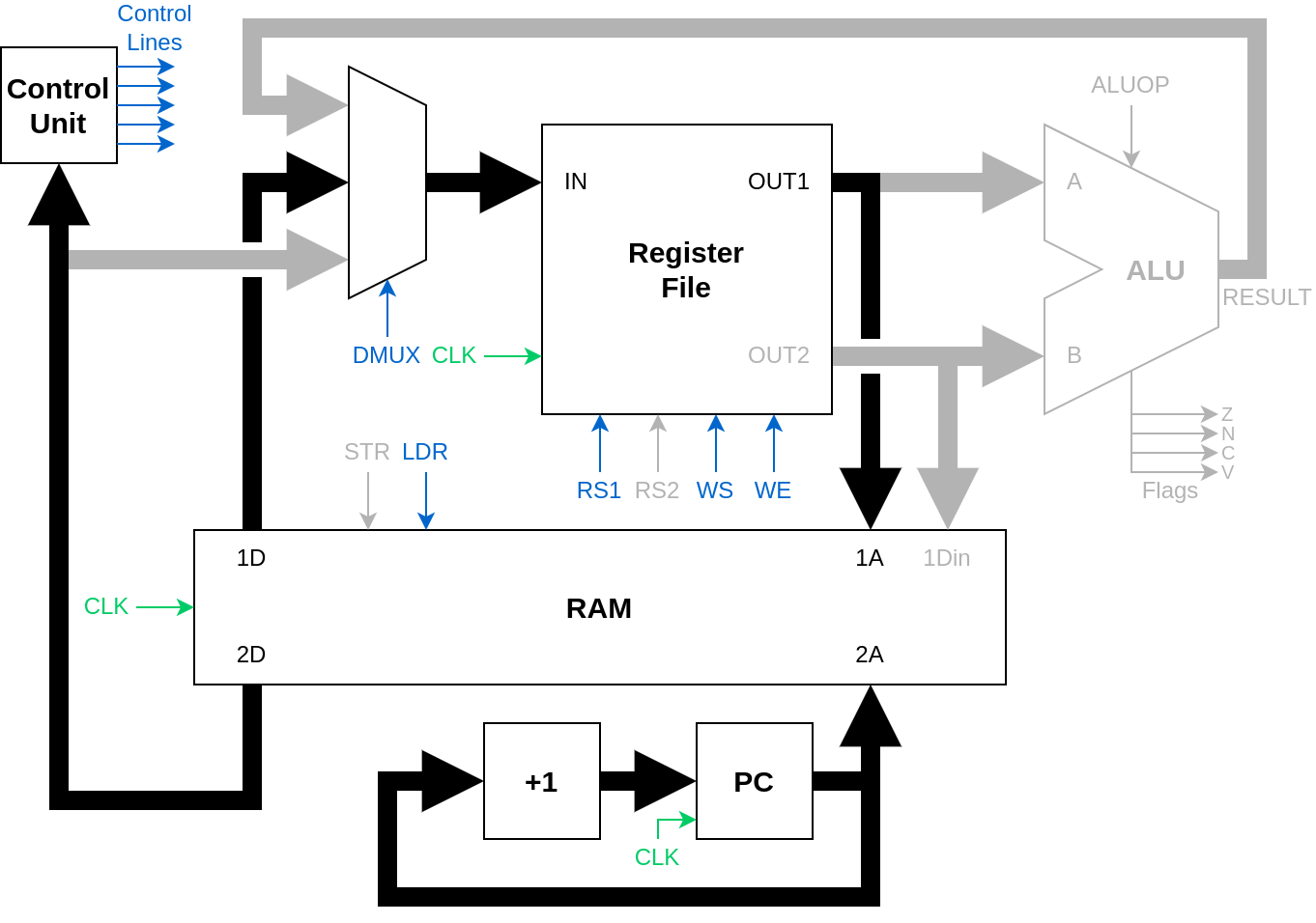
The str Instruction#
The register file outputs register <ra> to
the first address port on memory, and register <rd> to first data in
port on memory.
The store signal on memory is set to high, and the data is stored.
This is the only instruction where nothing is written back to a register,
so the register file does not write to any register.
 Storing data word to memory from register (str)
The movl Instruction#
The last (bottom) byte of the instruction is the 8-bit immediate value,
which is routed through the data multiplexer (DMUX = 10), and stored by the register
file in the destination register <rd>.
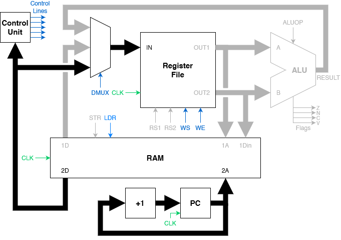 Moving an immediate value to a register (movl)
Exercise 1: Control Unit#
Your task is to build a circuit that receives
a single 16-bit input INST (representing an instruction)
and, based on the description above, sets the control lines appropriately.
For reference, the output control lines from the control unit are:
Control Signals#
-
ALUOP(2 bits) ALU Operation The function the ALU should perform, as defined in lab 2. Connects directly to the ALU. -
RS1(3 bits) Register Select 1 The first register to read from the register file, connects to the first Address slot on memory, as well as the A port on the ALU.
-
RS2(3 bits) Register Select 2 The second register to read from the register file, connects to the first Data slot slot on memory, as well as the B port on the ALU.
-
WS(3 bits) Write Select, the destination register to write a result back to.
-
WE(1 bit) Write Enable, allows the register file to be written to during execution of this instruction. -
STR(1 bit) Store, connected to thestrpin on memory, to tell the memory unit we are storing data to it.
-
LDR(1 bit) Load, connected to theldpin on memory, to tell the memory unit we are loading data from it.
-
DMUX(2 bit) Data Multiplexer, chooses which device is writing to the register file-
00Result from ALU writes to register file (add,sub,and,xor) -
01Data from memory writes to register file (ldr) -
10Instruction can write directly to register file (movl) -
11Undefined behavior (can just put a not connected component here)
-
Note that there are many “don’t-care” cases that can be used to simplify the design.
For instance, if the instruction to execute is a movl, then it doesn’t matter
what the RS1 and RS2 control lines are set to, nor does the ALUOP
value matter either, as the result from the ALU (or from memory) is ignored anyway.
In fact, one of the control lines is redundant (as it can
just always be set to HIGH). See if you can work out which one!
With control_unit.dig as a template, design and build a circuit that satisfies the
above description. Check your design against the included test for correctness.
The task appears quite tricky, but it is easily managed in steps. First, try to
write what each control line should be for each instruction. You can combine
the cases for all ALU instructions, as the four ALU instructions differ only in
the value of ALUOP, and all other control lines are the same. Try to include
as many “don’t-care” cases as possible. Simplify the truth table as much as
possible. Then, based on the table, come up with Boolean equations and finally
implement the logic circuit.
Exercise 2: Automatic CPU#
Now we have a functioning control unit; we can upgrade our manual CPU from last week into one that can execute instructions all on its own, by reading a list of instructions from memory.
Use cpu.dig as a template.
The dual-port memory is already present, as well as the program counter and the hardware to increment the program counter every cycle.
Your task:
-
Copy over the contents of
manual_cpu.dig, and replace the single-port memory with the dual-port memory shown, following the diagram provided. (You must make sure thatalu.digandreg_file.digare in the same directory.) -
Interface the control signals of the CPU with the outputs of the control unit. The control unit’s input port
INSTwill read data fromD2on the dual-port RAM component, at the address specified by the program counter. -
Replace the manual user input
INwith the valueimm8stored inside the instruction fetched from memory portD2. (You may need wire splitters.) Don’t forget to extend the value to 16 bits.
You may want to use tunnels (Components -> Wires -> Tunnel) to route the control signals, keeping the circuit tidy, similar to the diagrams above.
We do not advise the use of tunnels for main bus connections (like those that connect the major components of the CPU together). Draw them explicitly.
Do not replace the user input directly with D2, or executing a movl instruction
will bring the entire instruction into the register, not just the 8-bit immediate.
When executing movl r2, 0xAB, the machine code for this instruction is 0x02AB,
so we should have r2 := 0xAB, not r2 := 0x2AB. Do not forget that values written to registers need to be 16 bits wide.
Exercise 3: Assembly to Machine Code#
Now, the next step is to write a program for our CPU to execute.
We will start with something simple: A program that reads a number from
memory slot 0x9, adds one to it, and stores it back to memory.
We could write this in pseudo-code as
memory[0x9] = memory[0x9] + 1
Writing programs in machine code is very tedious and error prone, so usually we write programs in assembly language, and then translate the result into machine code. The assembly would look like this:
0. movl r1, 0x9    @ 0x0109
1. movl r2, 1
2. ldr r3, [r1]
3. add r3, r3, r2
4. str r3, [r1]
5. .word 0
6. .word 0
7. .word 0
8. .word 0
9. .word 0xFF
The end result is that memory slot 0x9 should now contain the value 0xFF + 1 = 0x100.
To run this program, we need to turn it into machine code, and then insert the machine code into memory.
Assemble the above program by hand into machine code, written as a series of 16-bit hexadecimal numbers. The first instruction has been assembled for you in the comment.
Here is a converter to help you out:
| Decimal | |
| Hex | |
| Binary |
Can you see why we spaced out the reserved bits now?
Exercise 4: Running My First Program#
Start the simulation, then:
- Right-click on the RAM component and store the machine code of the above program
in memory, starting from address
0x0000. - Open the measurement table and memory viewer.
- Toggle the clock line (tap c on the keyboard, or click the clock input) to watch the computer execute the program.
- Keep track of the registers (via the measurement table) and of RAM while the program executes.
- When the program counter gets to 5, you should see
the data in memory slot
0x9change from0xFFto0x100.
If the program did not execute correctly, it could be due to a few things:
- You made a mistake translating the assembly code to machine code.
- You have not loaded the machine code into memory correctly.
- Your CPU has a hardware bug (faulty logic). It is a good idea to think about what state the CPU should be in when executing an instruction, and then probe (Components -> IO -> Probe) the machine to make sure it’s doing the right thing.
How does the computer know which values in memory represent data, and which represent instructions? What would happen if we executed the code
0. .word 0x109   @ ???
1. ldr r2, [r1]
Conclusion#
At this point, we have a simple CPU that executes instructions given to it, one at a time. Unfortunately, there is no easy mechanism by which we can get the CPU to repeat the same set of instructions repeatedly in a loop. Loops and conditional execution is critical for solving many real-world problems. Next week we will upgrade our CPU to have this ability.
Push all your work to GitLab
-
All instruction in QuAC except for
strwrite a result to a destination register.strusesrdas the data to store to memory. While a little confusing, this makes the implemention in hardware a bit easier to deal with. ↩